Ferroelectric device and method for making

a ferroelectric device and making technology, applied in the direction of fixed capacitor details, fixed capacitor terminals, fixed capacitors, etc., can solve the problems of feram only being implemented, reducing the reliability of feram, and unable to achieve feram, so as to improve fatigue performance, reduce the thickness of amorphous layer, and improve the effect of electric fatigue performan

Inactive Publication Date: 2005-07-05
MACRONIX INT CO LTD
View PDF16 Cites 7 Cited by
  • Summary
  • Abstract
  • Description
  • Claims
  • Application Information

AI Technical Summary

Benefits of technology

[0008]The present invention may provide several advantages over conventional structures. By using a conductive perovskite LaNiO3 (LNO) bottom electrode as a seed layer, the crystallization temperature of in-situ sputter deposited PZT has been greatly reduced from about 600° C. to about 350° C. to 400° C. LNO has the same crystal structure as PZT with small (<5%) lattice mismatch. LNO's near-perfect lattice match with PZT allows PZT to growth epitaxially at low temperature. The 2Pr value of the low temperature grown PZT is about 20 C/cm2, and this provides 130 mV-400 mV sense margin when bit line capacitance is 800...

Problems solved by technology

However, the plasma and hydrogen-containing atmospheres used in CMOS interconnect processes damage the ferroelectric capacitor and decrease the reliability of FeRAM (Takashi Hase, Takehiro Noguchi and Yoichi Miyasaka, “Analysis of The Degradation of PZT and SrBi2TaO9 Thin Films with A Reductive Process,” Integrated Ferroelectric, 16, pp.
However, since interconnect...

Method used


Image

  • Ferroelectric device and method for making
  • Ferroelectric device and method for making
  • Ferroelectric device and method for making

Examples


Embodiment Construction

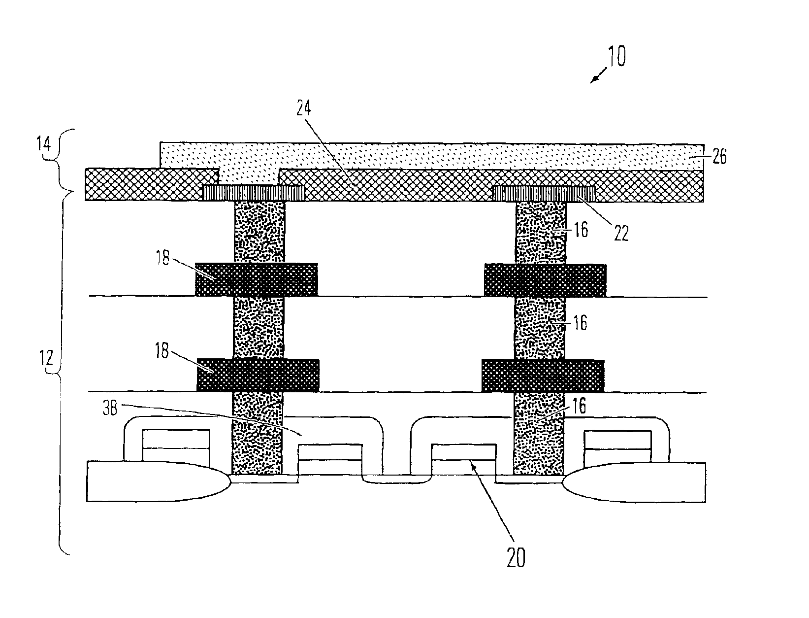
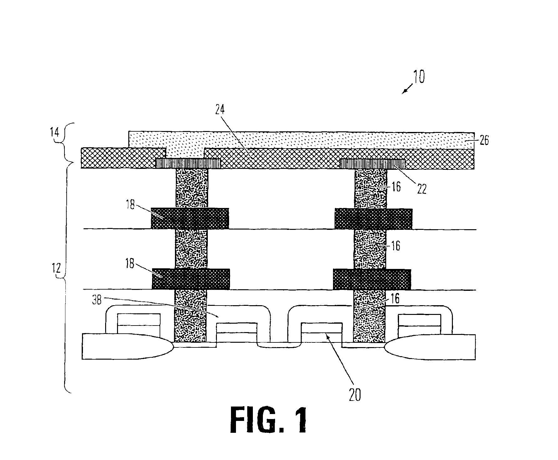
[0013]FIG. 1 illustrates a ferroelectric capacitor memory device 10 to include an IC layer 12, typically a CMOS IC layer, and a ferroelectric subassembly 14. IC layer 12 comprises contact plugs 16, interconnect lines 18, and pass transistor 20 electrically coupled to ferroelectric subassembly 14 through contact plugs 16 and lines 18. The construction of IC layer 12 may be conventional.

[0014]Ferroelectric subassembly 14 includes first, second and third layers 22, 24 and 26 formed upon the IC layer 12. First and third layers 22, 26 comprise first and second capacitor electrodes while second layer 24 is made of a ferroelectric material. The deposition of first layer 22 also creates contact 23 and Dad 44 (shown in FIG. 3). First and second capacitor electrodes 22, 26 are preferably made of LaNiO3 (LNO). Second layer 24 may comprise lead zirconate titanate (PZT), or lead lanthanum zirconate titanate (PLZT), or SrBi2TaO9 (SBT), or an appropriate combination thereof. Other ferroelectric ma...


PUM


Abstract

A ferroelectric subassembly for an integrated circuit includes a second layer lying between and in contact with first and third layers. The second layer comprises a ferroelectric material while the first and third layers comprise capacitor electrodes in contact with the second layer. At least a portion of the first layer contacting the second layer has the same crystal structure as the second layer. The first layer acts as both a seed layer for the ferroelectric material and as a capacitor electrode. One or both of the first and third layers may comprise LaNiO3 (LNO). The second layer may, for example, comprise lead zirconate titanate (PZT), lead lanthanum zirconate titanate (PLZT) or SrBi2TaO9 (SBT) or an appropriate combination thereof. Any lattice mismatch between the first and second layers and/or between the second and third layers may be less than about 5 percent.

Description

CROSS-REFERENCE TO RELATED APPLICATION[0001]This application is related to a copending patent application Ser. No. 10 / 270,997, filed on the same day as this application and having the same assignee, entitled “Ferroelectric Capacitor Memory Device Fabrication Method”.BACKGROUND OF THE INVENTION[0002]Computer memories may be classified as either volatile, that is memories that lose their stored information when power is removed, or non-volatile, that is memories that retain their stored information when power is removed. One type of nonvolatile memory uses a ferroelectric dielectric layer within the device. The direction of polarization of these ferroelectric capacitor memory devices, commonly called FeRAM, is used to determine its binary storage state.[0003]FeRAM is considered an ideal memory because of its low power consumption, low operation voltage, high writing speed and high endurance. Traditionally, the ferroelectric capacitor is fabricated before the CMOS interconnect process ...

Claims


Application Information

Patent Timeline
IPC IPC(8): H01L21/02H01L21/8246H01L27/115
CPCH01L27/11502H01L27/11507H01L28/55H10B53/30H10B53/00
Inventor LUNG, HSIANG-LAN
Owner MACRONIX INT CO LTD
Why Eureka
Try Eureka