Register controlled DLL for reducing current consumption

a technology of register control and current consumption, applied in the field of delay locked loop (dll), can solve the problems of increasing power consumption, time delay (or clock skew), and increasing power consumption, and achieve the effect of reducing current consumption

Inactive Publication Date: 2005-07-05
SK HYNIX INC
View PDF28 Cites 48 Cited by
  • Summary
  • Abstract
  • Description
  • Claims
  • Application Information

AI Technical Summary

Benefits of technology

[0015]It is, therefore, an object of the present invention to provide a register control delay locked loop capable of reducing current consumption caused by an unnecessary toggling of a DLL clock signal and to provide a semiconductor memory device having the same.

Problems solved by technology

When a clock signal from an external circuit is used in an internal circuit, a time delay (or clock skew) is generated.
Accordingly, this continuous toggling of the DLL clock increases power consumption and, specifically, this power consumption is much higher at high frequency operations.
However, since the size of the repeater 1 is relatively large, a large amount of current is consumed by the repeater 1.
Accordingly, when the DLL clock signal is continuously toggled, the current consumption of the peripheral circuits increases significantly.

Method used


Image

  • Register controlled DLL for reducing current consumption
  • Register controlled DLL for reducing current consumption
  • Register controlled DLL for reducing current consumption

Examples


Embodiment Construction

[0029]Hereinafter, a register controlled DLL in DDR SDRAM devices according to the present invention will be described in detail in reference with the accompanying drawings. A “unit” in the present invention is not necessarily a single entity, but can be composed of multiple components.

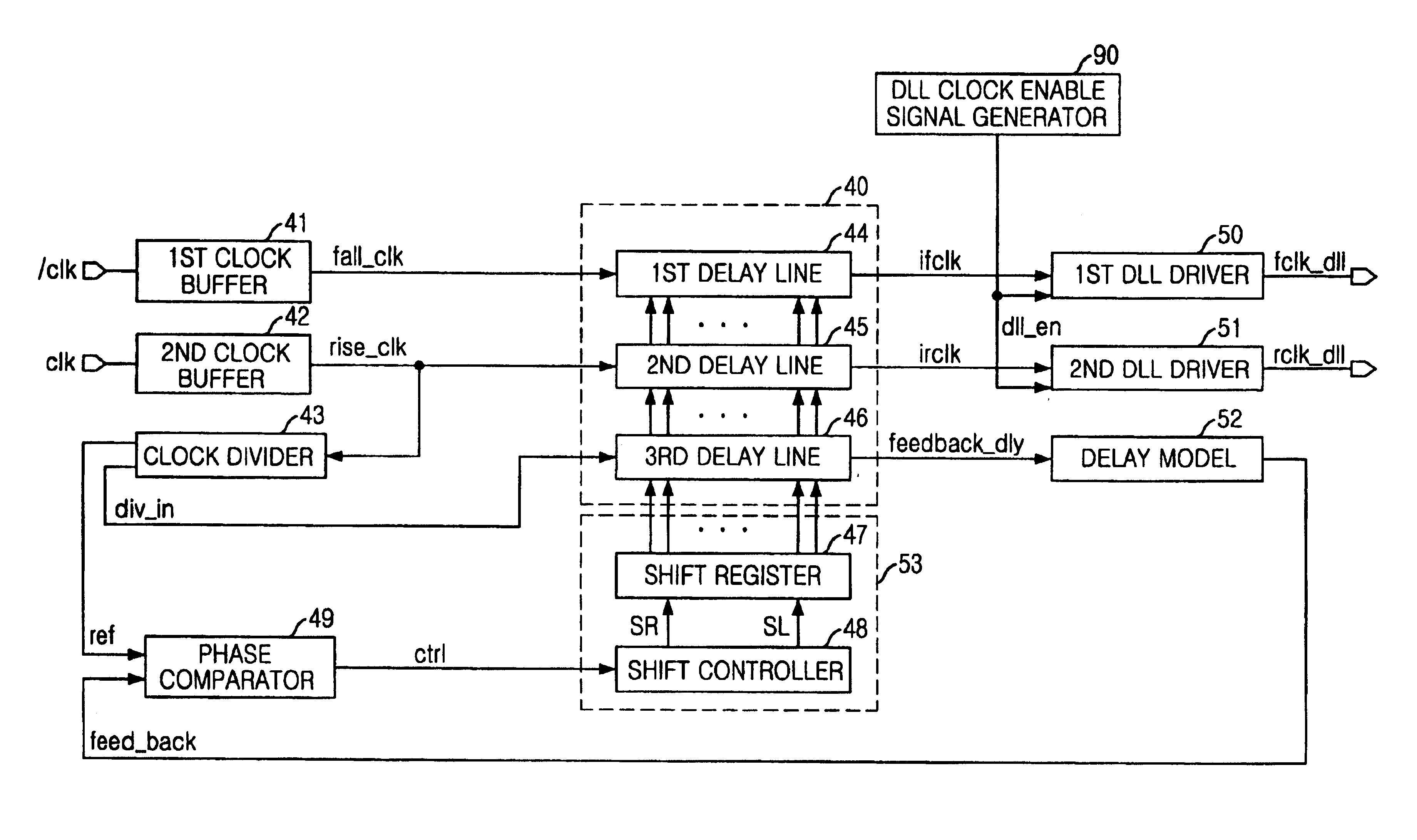
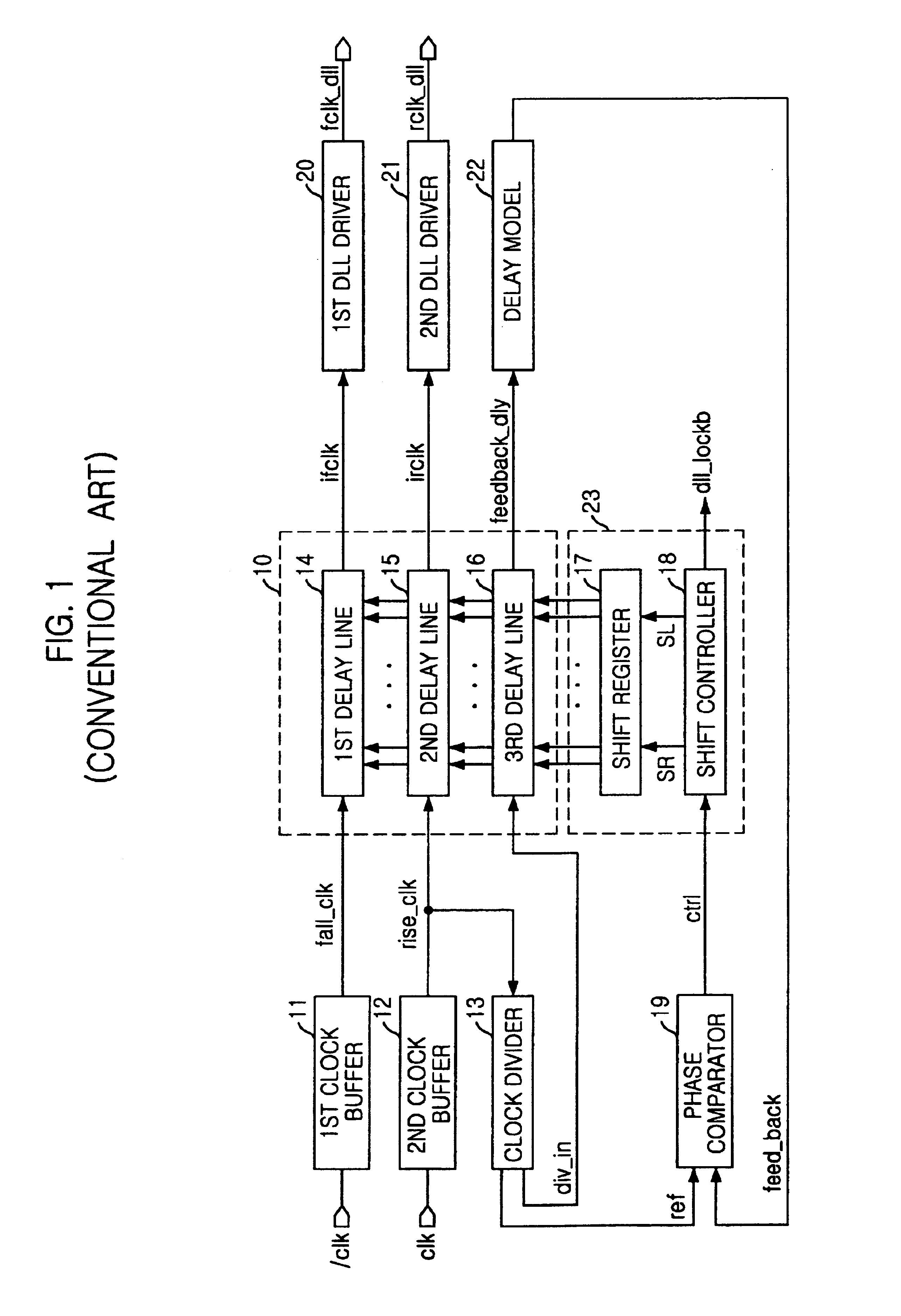
[0030]Referring to FIG. 4, the register control DLL according to an embodiment of the present invention includes first and second clock buffers 41 and 42, a clock divider 43, a phase comparator 49, a delay unit 40 which has first to third delay lines 44 to 46, a delay monitor 53 having a shift register 47 and a shift controller 48 in a DLL loop, first and second DLL drivers 50 and 51, and a delay model 52, all operatively coupled. The register control DLL shown in FIG. 4 has the same configuration as the DLL shown in FIG. 1, except for the addition of a DLL clock enable signal generator 54, first and second clock controllers 55 and 56 and connections resulting therefrom. Accordingly, the detailed desc...


PUM


Abstract

A register controlled delay locked loop (DLL) usable in a semiconductor device is provided. The register controlled delay locked loop includes an internal clock generating unit generating a delayed clock signal and a reference clock signal, a first delay unit compensating for an amount of delay caused by a signal transmission path of the delayed clock signal, a phase comparator detecting a difference between the reference clock signal and the delayed clock signal and thereby generating a detection signal, a controller having a plurality of second delay units for controlling an amount of delay of the delayed clock signal in response to the detection signal, a driver driving a DLL clock signal, and an enable signal generator enabling the driver in response to an activation or non-activation signal of the semiconductor device.

Description

[0001]This application is a divisional application of U.S. application Ser. No. 10 / 183,666 filed Jun. 28, 2002 (now U.S. Pat. No. 6,768,690 B2 issued on Jul. 27, 2004), for which priority is claimed under 35 U.S.C. §120; and the present application claims, under 35 U.S.C. §119, the priority benefit of Korean Patent Application No. 2001-38872 filed Jun. 30, 2001. The contents of each of these applications are herein fully incorporated by reference.BACKGROUND OF THE INVENTION[0002]1. Field of the Invention[0003]The present invention relates to a delay locked loop (DLL) in a semiconductor memory device and, more particularly, to a register controlled DLL capable of reducing current consumption by operating the DLL loop when the semiconductor device is only at an operation mode.[0004]2. Discussion of the Related Art[0005]Generally, in system circuits of semiconductor devices, a clock signal has been used as a reference signal for adjusting operation timing or guaranteeing a high-speed o...

Claims


Application Information

Patent Timeline
Patent Type & Authority Patents(United States)
IPC IPC(8): G11C7/00G11C7/22H03K5/13H03L7/081H03L7/08H03K5/00G06F1/10G11C11/407G11C11/4076
CPCG11C7/22G11C7/222H03K5/131H03L7/0802H03L7/0805H03L7/0814H03K2005/00058H03K2005/00104G11C11/407
Inventor KWON, KI-SEOPLEE, SEONG-HOON
Owner SK HYNIX INC
Why Eureka
Try Eureka