Low fabrication cost, high performance, high reliability chip scale package

a chip scale and low fabrication cost technology, applied in the direction of printed circuit aspects, conductive pattern reinforcement, conductive pattern formation, etc., can solve the problems of limit electrical performance and more serious impact on high frequency device performance, and achieve the effect of minimizing damage and high bump reliability

Inactive Publication Date: 2005-07-12
QUALCOMM INC
View PDF7 Cites 103 Cited by
  • Summary
  • Abstract
  • Description
  • Claims
  • Application Information

AI Technical Summary

Benefits of technology

[0011]A principle objective of the invention is to provide a high-pillar solder bump that sustains a high stand-off of the complete solder b...

Problems solved by technology

Limitations that are imposed on this method of packaging are typically limitations of electrical performance that is imposed on the device by the packaging interface.
For instance, of key concerns are RC delays in the transmission of signals over the various interconnect traces.
Also of concern are considerations of parasitic capacitance and inductance that ar...

Method used


Image

  • Low fabrication cost, high performance, high reliability chip scale package
  • Low fabrication cost, high performance, high reliability chip scale package
  • Low fabrication cost, high performance, high reliability chip scale package

Examples


Embodiment Construction

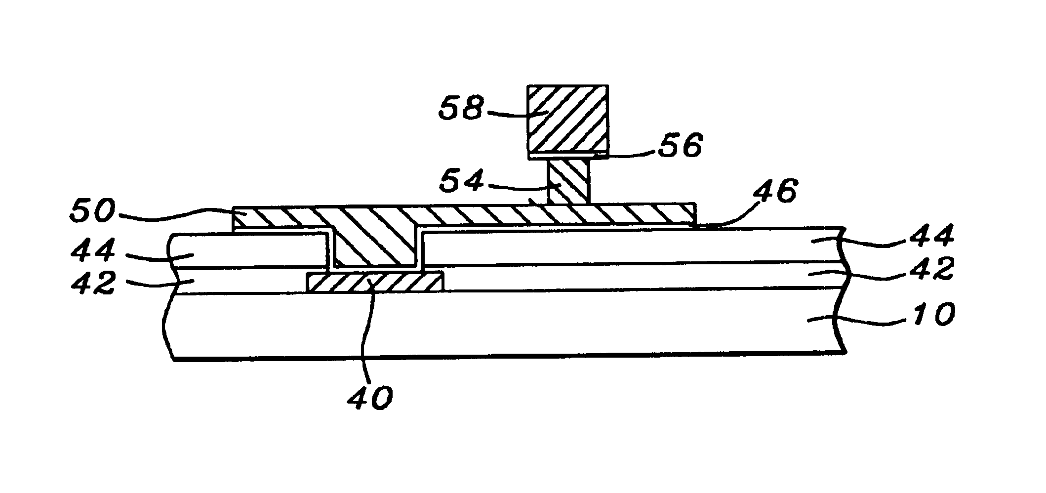
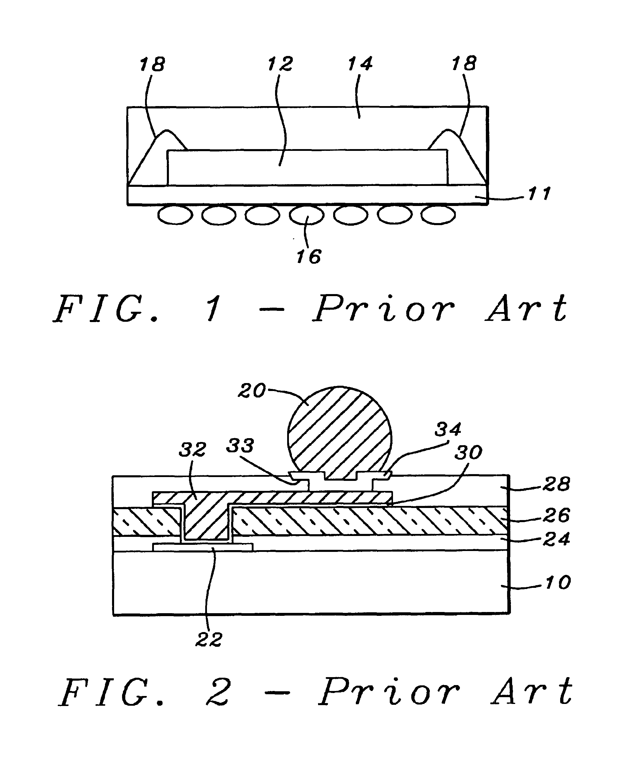
[0032]Two prior art applications are shown in the cross sections of FIGS. 1 and 2, specifically in the cross section of FIG. 1 are shown:[0033]11, a BGA substrate such as a printed circuit board and the like[0034]12, a semiconductor device or die[0035]14, a molding compound that is used to encapsulate the die 12[0036]16, solder balls that form the electrical interface between the package shown in cross section in FIG. 1 and surrounding circuitry; these solder balls can for instance be further connected to contact pads on the surface of a Printed Circuit Board (PCB)[0037]18, bond wires used to connect points of electrical contact (not shown) on the active surface of die 12 with contact pads (not shown) on the second or upper surface of BGA substrate 11.

[0038]FIG. 2 shows a cross section of a conventional re-routing bump, the re-routing applies since the solder bump that is shown in cross section in FIG. 2 does not align with the contact pad with which the solder bump is connected. Th...


PUM


Abstract

The invention provides a new method and chip scale package is provided. The inventions starts with a substrate over which a contact point is provided, the contact point is exposed through an opening created in the layer of passivation and a layer of polymer or elastomer. A barrier/seed layer is deposited, a first photoresist mask is created exposing the barrier/seed layer where this layer overlies the contact pad and, contiguous therewith, over a surface area that is adjacent to the contact pad and emanating in one direction from the contact pad. The exposed surface of the barrier/seed layer is electroplated for the creation of interconnect traces. The first photoresist mask is removed from the surface of the barrier/seed layer. A second photoresist mask, defining the solder bump, is created exposing the surface area of the barrier/seed layer that is adjacent to the contact pad and emanating in one direction from the contact pad. The solder bump is created in accordance with the second photoresist mask, the second photoresist mask is removed from the surface of the barrier/seed layer, exposing the electroplating and the barrier/seed layer with the metal plating overlying the barrier/seed layer. The exposed barrier/seed layer is etched in accordance with the pattern formed by the electroplating, reflow of the solder bump is optionally performed.

Description

[0001]This is a division of patent application Ser. No. 09 / 953,525, filing date Sep. 17, 2001 now U.S. Pat. No. 6,642,136, Low Fabrication Cost, High Performance, High Reliability Chip Scale Package, assigned to the same assignee as the present invention.BACKGROUND OF THE INVENTION[0002](1) Field of the Invention[0003]The invention relates to the fabrication of integrated circuit devices, and more particularly, to a method and package for semiconductor devices.[0004](2) Description of the Prior Art[0005]The creation of semiconductor devices, also referred to as Integrated Circuits (IC) has been made possible by the rapid development of supporting technologies such as photolithography and methods of etching. Most of these technologies have over the years had to address concerns created by a continued decrease in device dimensions and increase in device densities. This effort of creating improved performance devices does is not limited in its impact on the device itself but extends in...

Claims


Application Information

Patent Timeline
IPC IPC(8): H01L21/60H01L23/28H01L23/31H01L21/02H01L23/485H01L23/48H05K3/34H01L21/56H01L21/44H01L23/525H04B1/707H04B7/26H05K3/10H05K3/24
CPCH01L21/563H01L23/3114H01L23/3128H01L23/525H01L24/11H01L24/12H01L24/16H05K3/3473H01L21/565H01L2224/0401H01L2224/0231H01L2224/02311H01L2224/03912H01L2224/11462H01L2224/1147H01L2224/11831H01L2224/11849H01L2224/11901H01L2224/13023H01L2224/131H01L2224/48227H01L2224/73203H01L2924/01002H01L2924/01013H01L2924/01018H01L2924/01022H01L2924/01029H01L2924/01042H01L2924/01073H01L2924/01074H01L2924/01075H01L2924/01078H01L2924/01079H01L2924/04941H01L2924/09701H01L2924/14H01L2924/15311H01L2924/30105H01L2924/30107H04B1/712H05K3/108H05K3/243H05K2201/0367H05K2201/09436H05K2201/0949H05K2203/043H05K2203/054H01L2924/014H01L2924/01084H01L2924/01041H01L24/48H01L2924/00013H01L2924/01005H01L2924/01006H01L2924/01024H01L2924/01033H01L2224/13099H01L2924/351H01L2924/181H01L2224/05599H01L2224/45099H01L2224/85399H01L2924/00014H01L2224/13017H01L2924/00H01L2224/45015H01L2924/207H01L2924/00012
Inventor LEE, JIN YUANLEI, MING TAHUANG, CHING-CHENGLIN, CHUEN-JYE
Owner QUALCOMM INC
Why Eureka
Try Eureka