Reduction of capacitive effects in a semiconductor memory device

a technology of capacitive effects and memory devices, which is applied in the direction of semiconductor devices, digital storage, instruments, etc., can solve the problems of increasing coupling noise, and achieve the effect of reducing the coupling noise between interconnections without increasing the area of memory cells

Active Publication Date: 2005-07-12
RENESAS ELECTRONICS CORP
View PDF11 Cites 24 Cited by
  • Summary
  • Abstract
  • Description
  • Claims
  • Application Information

AI Technical Summary

Benefits of technology

[0009]An object of the present invention is to provide a semiconductor memory device allowing coupling noise between interconnections to be reduced without increasing a memory cell area.

Problems solved by technology

Therefore, the coupling capacitance between interconnections may cause crosstalk, resulting in a malfunction.
If the shielding interconnection is not provided, the increased coupling capacitance between word lines as described above increases the coupling noise, which causes a malfunction.

Method used


Image

  • Reduction of capacitive effects in a semiconductor memory device
  • Reduction of capacitive effects in a semiconductor memory device
  • Reduction of capacitive effects in a semiconductor memory device

Examples


first embodiment

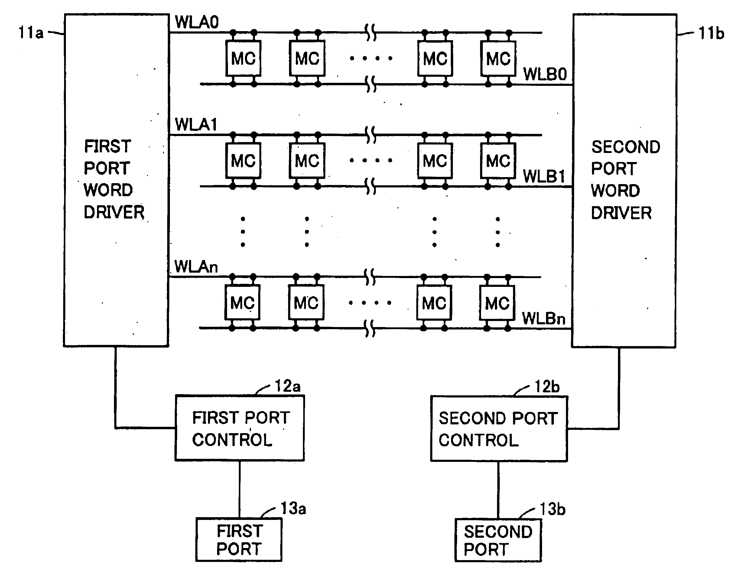
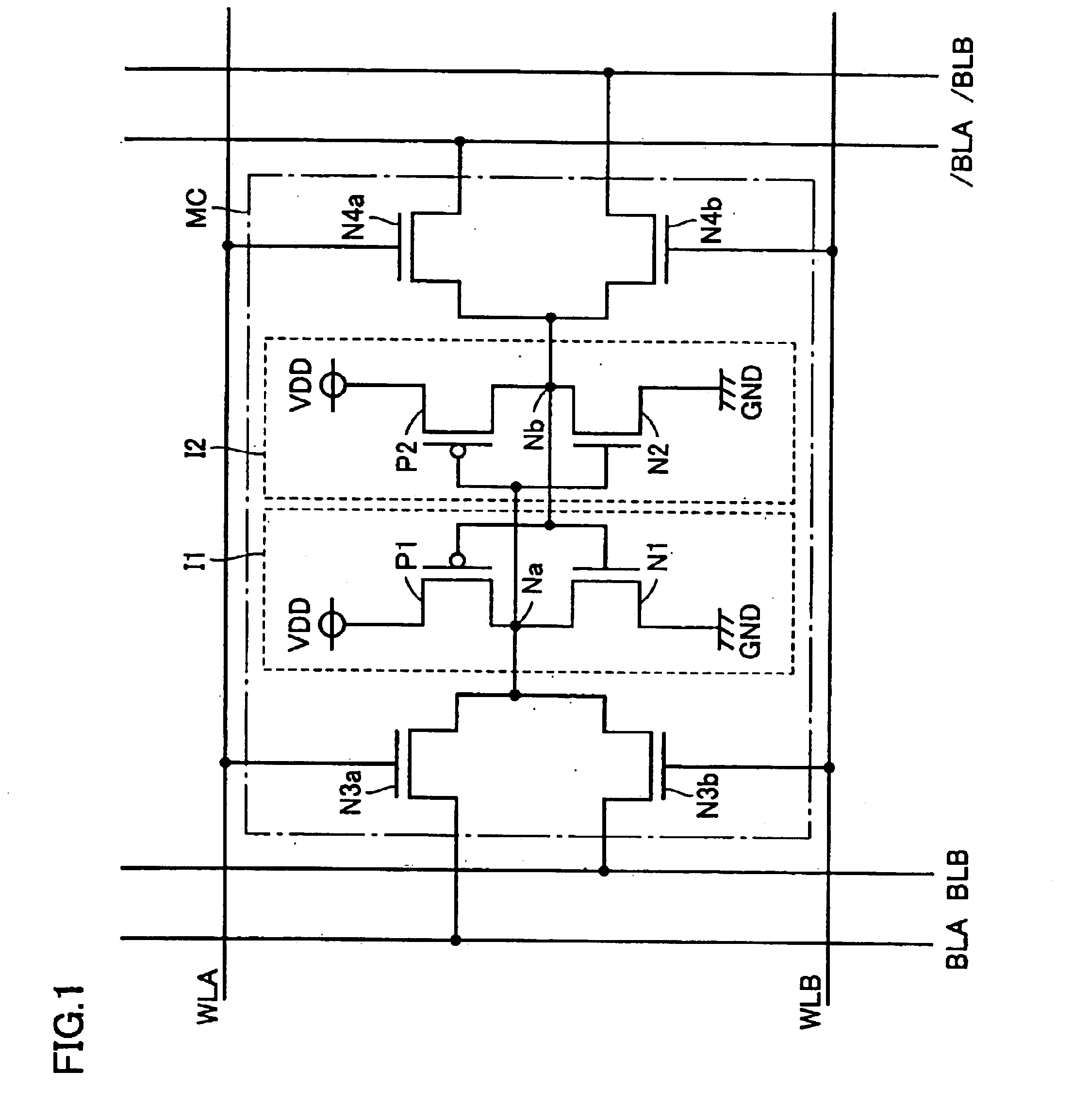
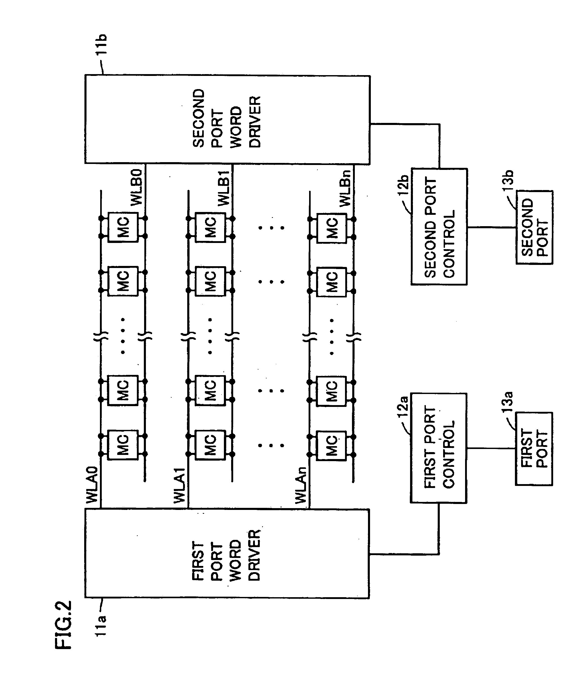
[0040](First Embodiment)

[0041]Referring to FIG. 1, memory cell MC has two driver transistors N1, N2, two load. transistors P1, P2, and four access transistors N3a, N3b, N4a, N4b.

[0042]Each of two driver transistors N1, N2, and four access transistors N3a, N3b, N4a, N4b is formed of an NMOS transistor, and each of two load transistors P1, P2 is formed of a pMOS transistor.

[0043]NMOS transistor N1 and pMOS transistor P1 constitute a first CMOS (Complementary Metal Oxide Semiconductor) inverter I1, and nMOS transistor N2 and pMOS transistor P2 constitute a second CMOS inverter I2. A flip-flop circuit and storage nodes Na, Nb are formed by connecting the output terminal of one of first and second inverters I1 and I2 to the input terminal of the other.

[0044]The source of each of driver transistors N1, N2 is connected to a GND potential and the source of each of load transistors P1, P2 is connected to a VDD potential.

[0045]The source, gate, and drain of nMOS transistor N3a are connected ...

second embodiment

[0062](Second Embodiment)

[0063]In the present embodiment, an exemplary layout configuration to realize the word line arrangement in the first embodiment will specifically be described.

[0064]A layout configuration of memory cell MC1 of one bit will be described.

[0065]Referring mainly to FIG. 8, one n-type well region NW as well as two p-type well regions PW0, PW1 with the n-type well region NW interposed therebetween are formed on a surface of a semiconductor substrate. PMOS transistors P1, P2 are formed in n-type well NW. NMOS transistors N1, N3b, N4b are formed in p-type well PW0, and nMOS- transistors N2, N3a, N4a are formed in p-type well PW1.

[0066]PMOS transistor P1 has the source formed of a p-type diffusion region FL13, the drain formed of a p-type diffusion region FL14, and gate PL1. PMOS transistor P2 has the source formed of a p-type diffusion region FL11, the drain formed of a p-type diffusion region FL12, and gate PL2.

[0067]NMOS transistor N1 has the source formed of an n...

third embodiment

[0085](Third Embodiment)

[0086]In the present embodiment, a two-port SRAM memory cell with a read-only port, which is a different type from the first and second embodiments, will be described.

[0087]Referring to FIG. 11, this memory cell MC has two driver transistors N1, N2, two load transistors P1, P2, two access transistors N3, N4, and nMOS transistors N5, N6 constituting a read-only port.

[0088]Each of two driver transistors N1, N2, two access transistors N3, N4, and transistors N5, N6 is formed of an nMOS transistor, and each of two load transistors P1, P2 is formed of a pMOS transistor.

[0089]NMOS transistor N1 and PMOS transistor P1 constitute a first CMOS inverter I1, and NMOS transistor N2 and pMOS transistor P2 constitute a second CMOS inverter I2. A flip-flop circuit as well as storage nodes Na, Nb are formed by connecting the output terminal of one of first and second inverters I1, I2 to the input terminal of the other.

[0090]The source of each of driver transistors N1, N2 is ...


PUM


Abstract

A semiconductor memory device having a multiport memory includes a plurality of memory cells MC arranged in columns and rows, a plurality of first word lines WLA0-WLAn connected to a first port 13a, and a plurality of second word lines WLB0-WLBn connected to a second port 13b. Each of a plurality of first word lines WLA0-WLAn and each of a plurality of second word lines WLB0-WLBn are arranged alternately in a planar layout. A semiconductor memory device is thus obtained that allows a coupling noise between interconnections to be reduced without an increase in memory cell area.

Description

BACKGROUND OF THE INVENTION[0001]1. Field of the Invention[0002]The present invention relates to a semiconductor memory device, and more particularly to an SRAM (Static Random Access Memory) semiconductor memory device having a multiport memory or a content addressable memory.[0003]2. Description of the Background Art[0004]In multiport memory cells, bit lines or word lines of each port are often arranged adjacent to each other. Therefore, the coupling capacitance between interconnections may cause crosstalk, resulting in a malfunction.[0005]Japanese Patent Laying-Open No. 2000-12704, for example, proposes a method of avoiding interference of word lines with each other by providing GND interconnections for write word lines and read word lines. Similarly, Japanese Patent Laying-Open No. 2000-236029 proposes a method of avoiding interference between word lines by providing a GND interconnection between rows of memory cells adjacent to each other.[0006]Both of these approaches require a...

Claims


Application Information

Patent Timeline
Patent Type & Authority Patents(United States)
IPC IPC(8): G11C8/16G11C8/00G11C11/41H01L21/8244H01L27/108H01L27/11
CPCG11C8/16G11C5/063H10B12/00
Inventor NII, KOJI
Owner RENESAS ELECTRONICS CORP
Why Eureka
Try Eureka