Single substrate annealing of magnetoresistive structure

a single substrate and magnetoresistive technology, applied in the direction of substrate/intermediate layer, spin-exchange-coupled multilayer, inductance/transformer/magnet manufacturing, etc., can solve the problems of large, bulky structure for magnetic field generation, known bulk process, etc., to improve improve the effect of pinning uniformity and process control

Inactive Publication Date: 2005-07-19
MICRON TECH INC
View PDF3 Cites 8 Cited by
  • Summary
  • Abstract
  • Description
  • Claims
  • Application Information

AI Technical Summary

Benefits of technology

[0015]The present invention provides apparatus and processes for annealing individual wafers containing MRAM devices. A wafer is placed on a hot chuck and heated to the Néel temperature for the AF layer. A localized magnetic field generated by a permanent magnet or Helmholtz coil, for example, is applied to one wafer at a time as the wafer is cooled. The system allows for rapid heating and cooling of the wafer, and highly accurate and uniform temperature control. In addition, individual wafers can be cycled repeatedly to improve pinning uniformity and process control.

Problems solved by technology

Consequently, the known bulk processes have several disadvantages, including the need for long heating cycles (greater than an hour, and up to five hours, for 25 wafers, for example) and large, bulky structures for magnetic field generation.
One difficulty of a prolonged annealing process, such as the bulk process described above, is interdiffusion of the ultra-thin layers of the layered structure 30.
The build-up of manganese degrades the performance of the structure, for example, by disadvantageously diminishing the tunneling magnetoresistive (TMR) signal that otherwise would be generated by the device structure.
During the extra heating time, unwanted changes can occur in the MRAM devices being annealed, such as manganese ion migration noted above.
In addition, when entire devices are being heated during the annealing process, high annealing temperatures may have adverse effects on other materials in the devices.
Accordingly, prior art processing requirements can limit the types of materials to be used in fabrication of a magnetic memory element.
Further, in bulk processing, uniform magnetic field and heating parameters on individual wafers may be difficult to control.
This process unnecessarily subjects the entire packaged device to heating, such that only limited, heat-resistant materials can be used in the package.

Method used


Image

  • Single substrate annealing of magnetoresistive structure
  • Single substrate annealing of magnetoresistive structure
  • Single substrate annealing of magnetoresistive structure

Examples


Embodiment Construction

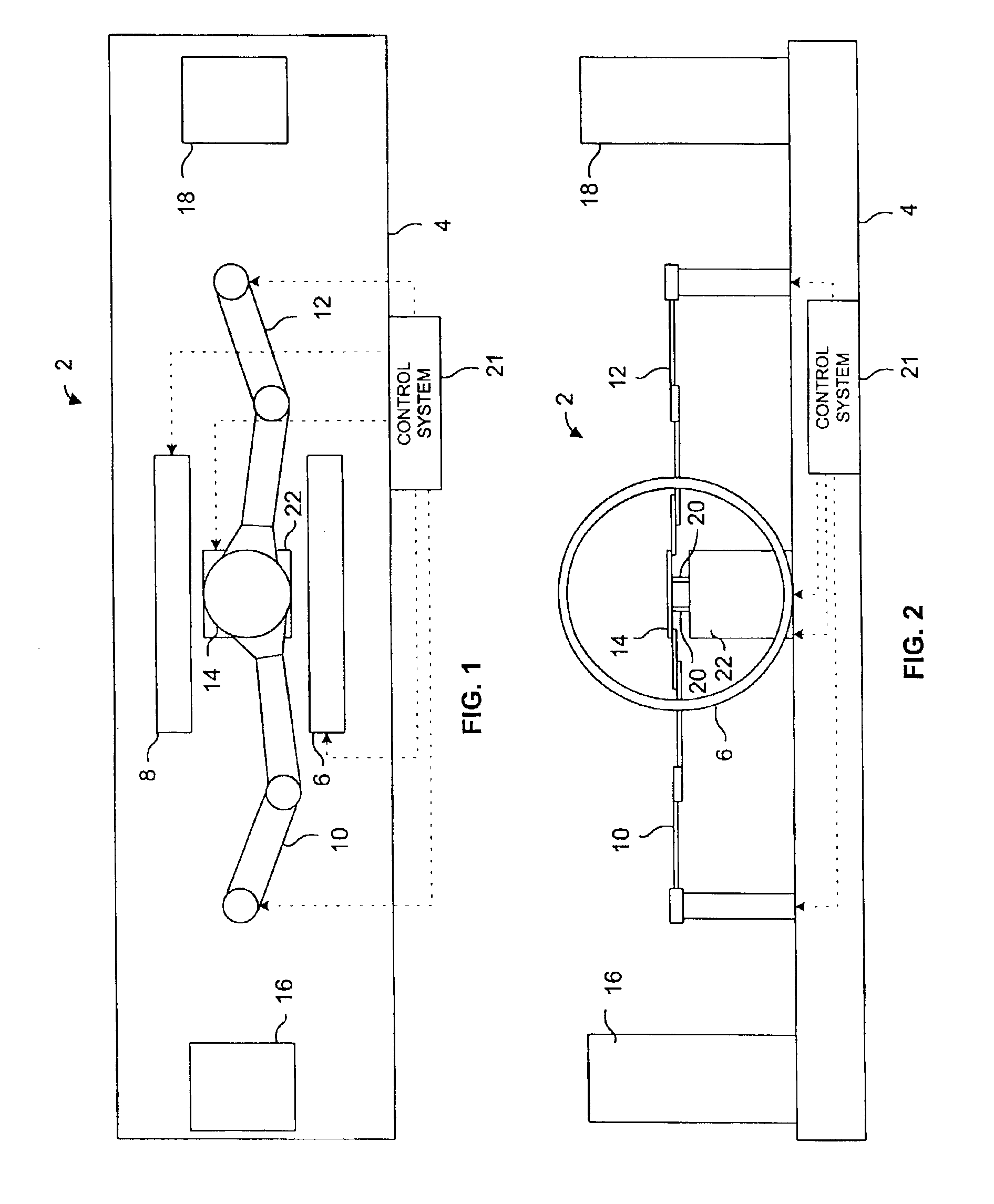
[0024]Referring initially to FIGS. 1 and 2, an apparatus 2 is shown for annealing wafers in a magnetic memory device fabrication process according to the present invention. Annealing apparatus 2 includes a base 4 which supports a Helmholtz coil made up of current loops 6 and 8. The ideal Helmholtz coil includes two coaxial circular current loops with the same radius, separated from each other by one radius. Alternatively, a permanent magnet, such as an alnico or ferrite magnet, for example, could be used in place of the Helmholtz coil, the magnet being positioned as necessary to provide an effective magnetic field. A pair of robotic arms 10 and 12 transports a wafer 14 from an input cassette 16 through the annealing apparatus to an output cassette 18.

[0025]As shown in FIG. 2, wafer 14 is supported on retractable pins 20 above a heated chuck 22. The chuck and associated heater are made of non-magnetic materials. Alternatively, the wafer can be heated by other methods, including radia...


PUM

PropertyMeasurementUnit
Néel temperatureaaaaaaaaaa

Abstract

A device for magnetically annealing magnetoresistive elements formed on wafers includes a heated chuck and a delivery mechanism for individually placing the wafers individually on the chuck one at a time. A coil is adjacent to the chuck and generates a magnetic field after the wafer is heated to a Néel temperature of an anti-ferromagnetic layer. A control system regulates the temperature of the heated chuck, the strength of the magnetic field, and a time period during which each chuck is heated to control the annealing process. The annealed elements are incorporated in the fabrication of magnetic memory devices.

Description

BACKGROUND OF THE INVENTION[0001]1. Field of the Invention[0002]The invention relates to magnetic annealing of fabricated magnetic random access memory (MRAM) elements, and more specifically to single substrate magnetic annealing of magnetic random access memory elements.[0003]2. Description of the Related Art[0004]Various types of electronic devices utilize ferromagnetic materials with defined magnetic properties. Among these are magnetic random access memory (MRAM) devices which contain arrays of magnetic memory elements formed using magnetic tunnel junction (MTJ) or giant magnetoresistance (GMR) principals. Operation of the memory elements depends in part on a pinned magnetic layer having a specific orientation of the magnetic field. The pinned magnetic layer is typically pinned by an antiferromagnetic (AF) layer having a specific magnetic field orientation. In a typical application, the pinning is effected by a thin layer (˜100 Å) of AF material, such as IrMn, adjacent a ferroma...

Claims


Application Information

Patent Timeline
Patent Type & Authority Patents(United States)
IPC IPC(8): H01F41/30H01F41/14
CPCB82Y25/00H01F1/0009H01F41/304B82Y40/00
Inventor TUTTLE, MARK E.WEIMER, RONALD A.
Owner MICRON TECH INC
Why Eureka
Try Eureka