Method and resulting structure for manufacturing semiconductor substrates

a technology of semiconductor substrates and manufacturing methods, applied in the direction of polycrystalline material growth, crystal growth process, chemically reactive gas, etc., can solve the problems of compound semiconductor wafers that compound semiconductor wafers are more prone to damage, and integrated circuits made from these semiconducting compounds are still relatively expensive compared to circuits, etc., to achieve a broader range of applicability

Inactive Publication Date: 2005-07-19
EPITACTIX PTY LTD
View PDF32 Cites 4 Cited by
  • Summary
  • Abstract
  • Description
  • Claims
  • Application Information

AI Technical Summary

Benefits of technology

[0021]According to the present invention, techniques for manufacturing substrates are provided. More particularly, the invention provides a method and device for improved semiconductor substrates to form advanced semiconductor devices. Merely by way of example, the invention has been applied to a metallic substrate that includes a plurality of panels and / or tiles, which are bonded on the substrate, for the manufacture of the advanced semiconductor devices. But, it would be recognized that the invention has a much broader range of applicability.

Problems solved by technology

Unfortunately, integrated circuits made from these semiconducting compounds are still relatively expensive compared to circuits made from silicon semiconductors.
This cost difference is largely attributable to the respective material costs, and wafer processing costs.
Other limitations also exist with compound semiconductor materials.
Compound semiconductor wafers are more prone to damage.
For example, they are more brittle than conventional single crystal silicon wafers.
Growing large crystal boules of compound semiconductor material is extremely difficult compared with growing large single crystal silicon boules.
Unfortunately, larger diameter wafers are difficult to make efficiently.
Even if larger boules of compound semiconductor material could be produced, handling the resulting large-diameter compound semiconductor wafers would generally be problematic.
Compound semiconductor wafers of the desired thickness and diameter would be extremely fragile and prone to breakage.
Here, the larger wafers would generally break due to the brittle nature of these semiconductor compounds.
Handling thinned compound semiconductor wafers is often difficult, and compound semiconductor wafers are commonly broken from step (iv) onwards.
Breakage is costly, since most of the processing (steps (i) to (iii)) is already complete.
The fragility of compound semiconductor materials also causes breakages of resulting chip devices, and restricts the larger size of practical chip designs that use compound semiconductor materials.
Here, larger sized compound semiconductor materials are not practical to make efficiently.

Method used


Image

  • Method and resulting structure for manufacturing semiconductor substrates
  • Method and resulting structure for manufacturing semiconductor substrates
  • Method and resulting structure for manufacturing semiconductor substrates

Examples


Embodiment Construction

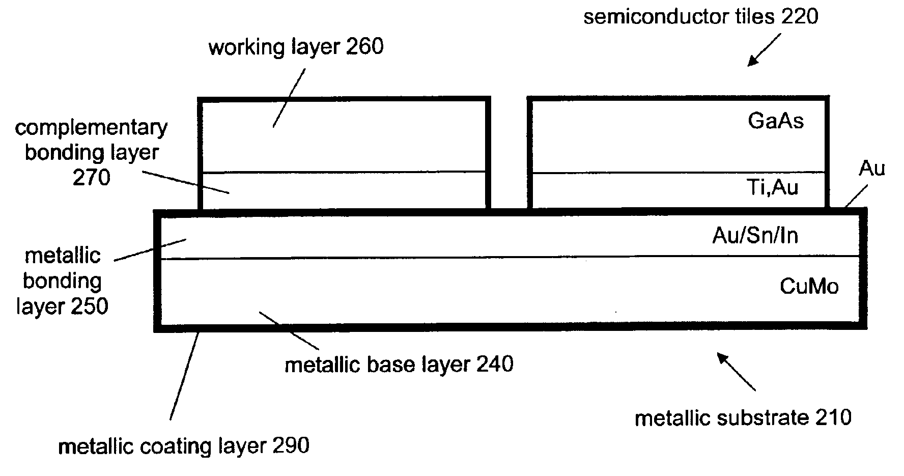
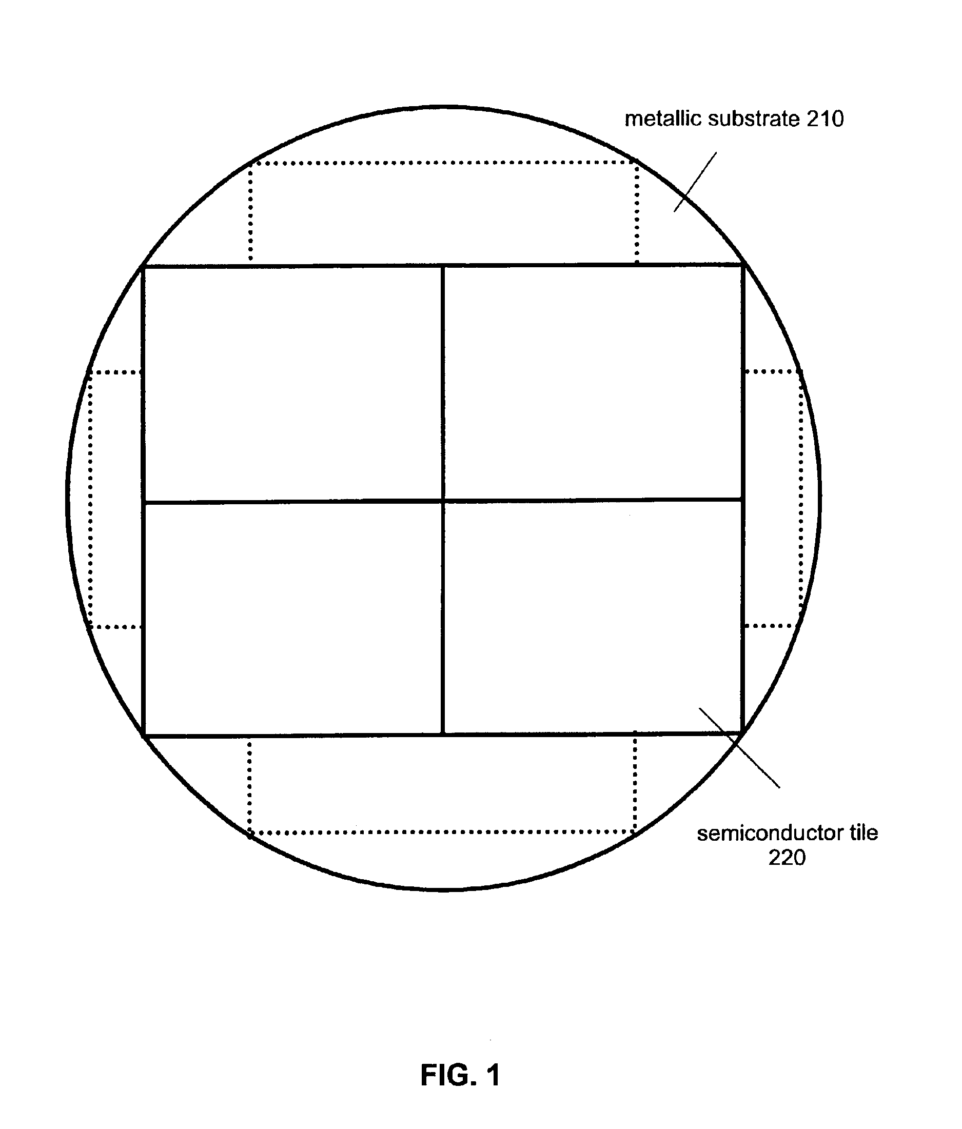
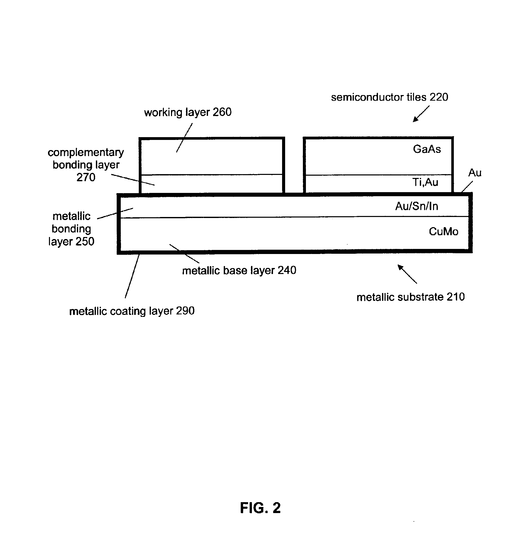
[0032]According to the present invention, techniques for manufacturing substrates are provided. More particularly, the invention provides a method and device for improved semiconductor substrates to form advanced semiconductor devices. Merely by way of example, the invention has been applied to a metallic substrate that includes a plurality of panels and / or tiles, which are bonded on the substrate, for the manufacture of the advanced semiconductor devices. But it would be recognized that the invention has a much broader range of applicability.

[0033]A semiconductor wafer composite is described herein. The composite is well suited to fabrication of compound semiconductor devices. Further, the composite has particular application in the context of large scale production of such devices. The semiconductor wafer composite from which the individual semiconductor devices are fabricated is first described, followed by a procedure for high volume production of semiconductor devices using the...


PUM

PropertyMeasurementUnit
diameteraaaaaaaaaa
diametersaaaaaaaaaa
diametersaaaaaaaaaa

Abstract

A semiconductor wafer composite is used as a basis for fabricating semiconductor chips, especially compound semiconductor devices. The semiconductor wafer composite advantageously comprises a metallic substrate 210 and multiple semiconductor tiles 220 bonded to the surface of the metallic substrate 210. The semiconductor wafer composite is effectively used as a single large semiconductor wafer for volume fabrication, and can be used to fabricate semiconductor devices in a similar manner.

Description

CROSS-REFERENCES TO RELATED APPLICATIONS[0001]This application claims priority to Australian Provisional Patent Application No. PS1122 filed Mar. 14, 2002, commonly assigned, and hereby incorporated by references for all purposes.STATEMENT AS TO RIGHTS TO INVENTIONS MADE UNDER FEDERALLY SPONSORED RESEARCH OR DEVELOPMENTBACKGROUND OF THE INVENTION[0002]The present invention relates generally to manufacturing substrates. More particularly, the invention provides a method and device for improved semiconductor substrates to form advanced semiconductor devices. Merely by way of example, the invention has been applied to a metallic substrate that includes a plurality of panels and / or tiles, which are bonded on the substrate, for the manufacture of the advanced semiconductor devices. But it would be recognized that the invention has a much broader range of applicability.[0003]As technology progresses, semiconductor manufacturers have continually strived to use ever larger wafers to obtain ...

Claims


Application Information

Patent Timeline
Patent Type & Authority Patents(United States)
IPC IPC(8): H01L21/00H01L23/544H01L23/14H01L23/12H01L21/70H01L21/78C30B23/00C30B25/00C30B28/12C30B28/14H01L21/20H01L21/301H01L21/304H01L21/44H01L21/46H01L21/48H01L21/50H01L21/60H01L21/768H01L23/373H01L23/492H01L23/552
CPCH01L23/544H01L21/0262H01L24/18H01L21/02425H01L24/97H01L21/02532H01L21/02546H01L21/4871H01L24/31H01L21/76898H01L24/82H01L23/3736H01L21/2003H01L23/492H01L21/78H01L23/142H01L24/83H01L23/552H01L2924/01006H01L2924/01023H01L2924/0132H01L2924/01079H01L2924/19043H01L2924/3025H01L2924/01061H01L2924/01033H01L2924/01078H01L2924/0105H01L2924/14H01L2924/01082H01L2924/01049H01L2924/01042H01L2224/18H01L2924/01322H01L2924/01029H01L2924/19042H01L2924/30107H01L2224/83801H01L2924/3011H01L2924/19041H01L2924/01005H01L2924/30105H01L2224/97H01L2224/8319H01L2924/10329H01L21/304H01L2224/82H01L2224/83H01L2924/12042H01L2224/92144H01L2924/00
Inventor CUNNINGHAM, SHAUN JOSEPH
Owner EPITACTIX PTY LTD
Why Eureka
Try Eureka