Stress accommodation in electronic device interconnect technology for millimeter contact locations

Inactive Publication Date: 2005-07-19
INVENSAS CORP
View PDF5 Cites 15 Cited by
  • Summary
  • Abstract
  • Description
  • Claims
  • Application Information

AI Technical Summary

Benefits of technology

[0010]The providing of an interface array of conductive joint members for use in forming an interconnecting interface between mating surfaces such as a pad on a surface mount electronic device and contacts on a circuit card where one portion of the conductive joint members are of a relatively elongated or oval outline and are oriented with the longer dimension in one direction to accommodate wiring spacing and another portion oriented in a different direction for accommodating expansion stress. In manufacturing when the relatively elongated shape is oriented with the longer dimension along the wiping motion di

Problems solved by technology

As a result, the distance between the pad connections of the device such as a semiconductor chip, and the wiring circuitry or printed circuit contact locations, where the device is attached to a wiring substrate, such as a printed circuit card, hereinafter the card, through conductive joints, becomes smaller and any expansion mismatch between the materials involved becomes more difficult to handle.
Such spacing imposes a severe constraint on the reliable wireability and long term reliability in service of fine pitched electronic devices.
Heretofore in the art there have been two major limitations in the formation of conductive joints when the size of the contacts approach one millimeter or less.
The first is that

Method used


Image

  • Stress accommodation in electronic device interconnect technology for millimeter contact locations
  • Stress accommodation in electronic device interconnect technology for millimeter contact locations
  • Stress accommodation in electronic device interconnect technology for millimeter contact locations

Examples


Embodiment Construction

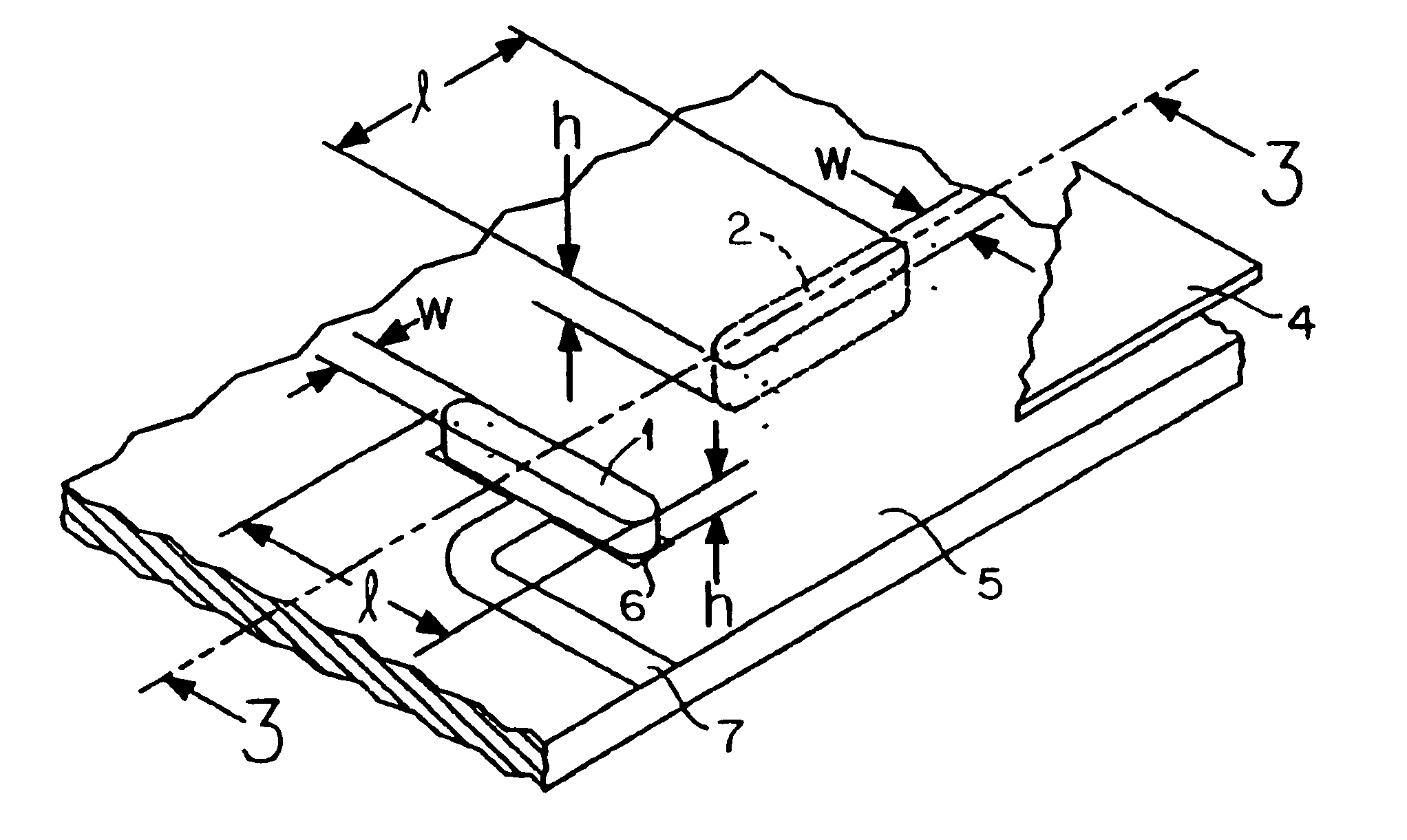
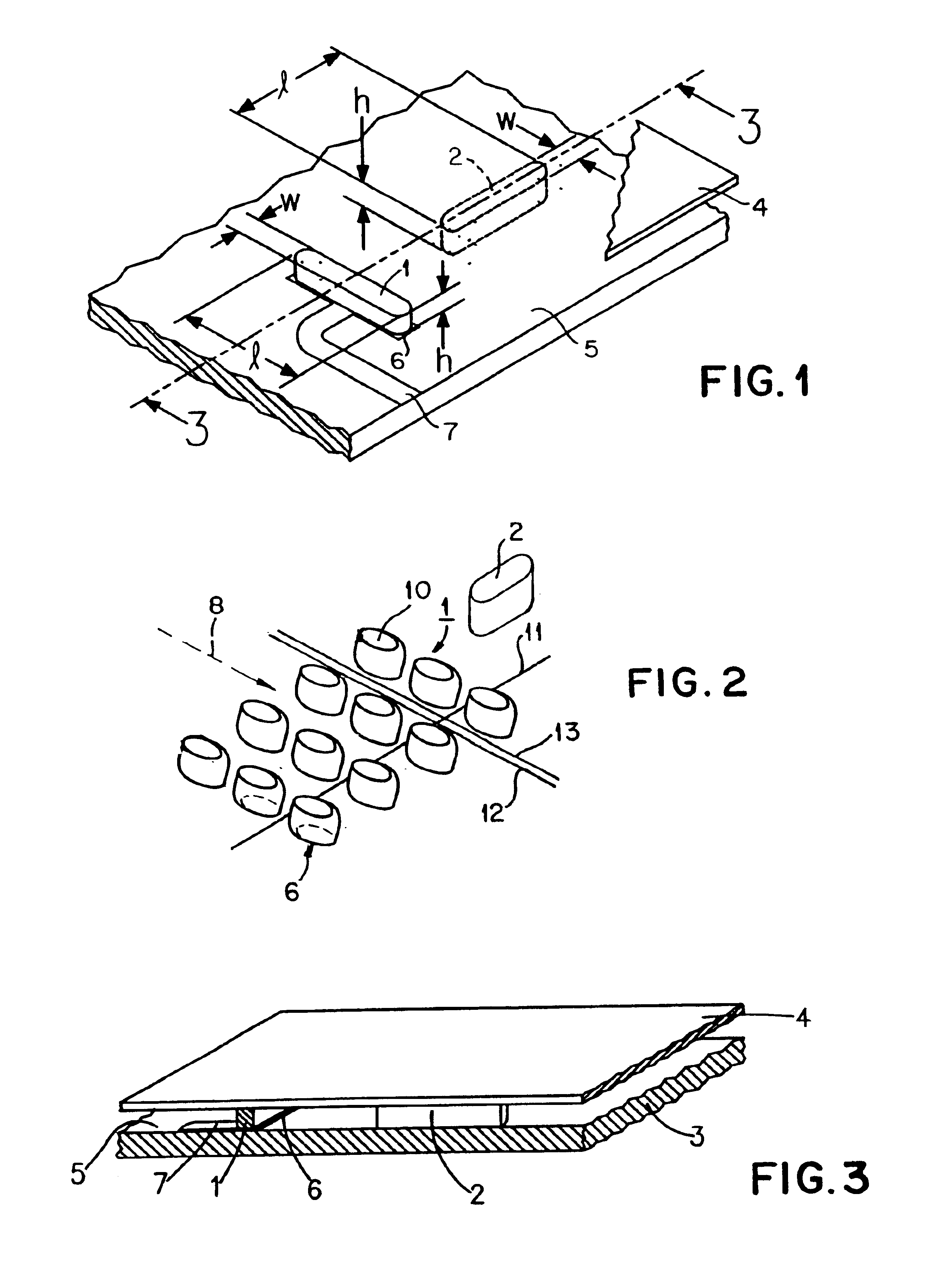
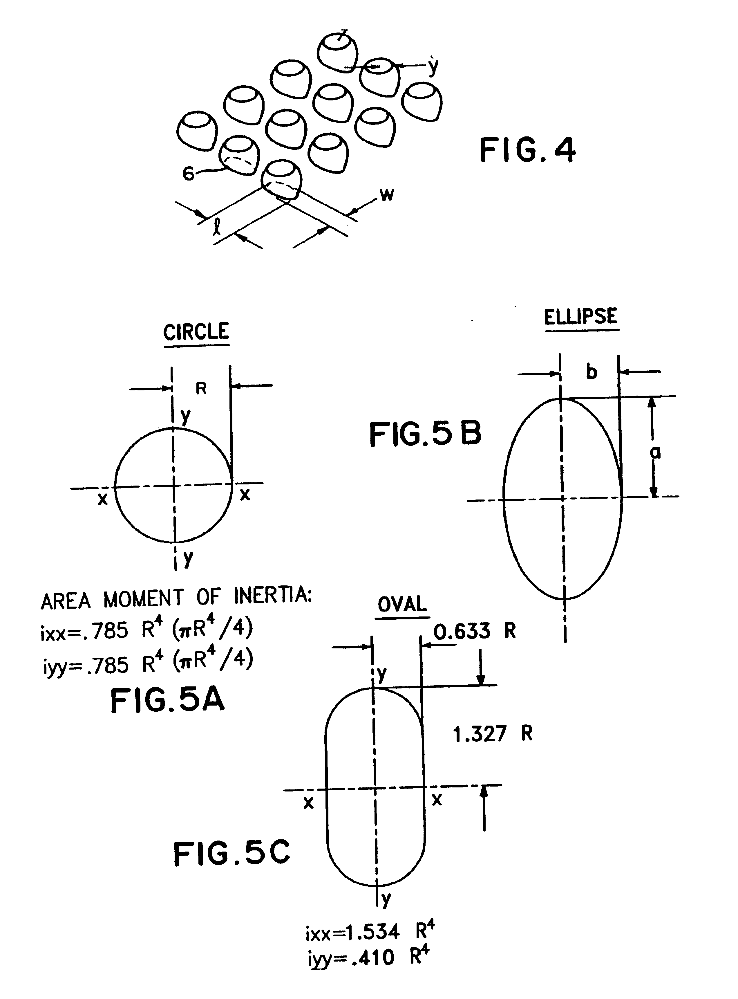
[0023]In accordance with the invention, in the formation of a screened conductive joint interface such as between mating surfaces of a pad on a surface mount electronic device and contacts on a wiring support member such as a printed circuit, when the pitch or centerline spacing becomes reduced to about a millimeter, expansion mismatch of the materials involved becomes a serious consideration and major benefits are achieved by using as an array interface an elongated or oval shape for the conductive joint member together with an expansion mismatch accommodating capability.

[0024]The interface of the invention may be viewed as having a contact spacing accommodation portion employing elongated conductive joints aligned to provide additional space to accommodate wiring and an expansion mismatch accommodation capability portion arranged to offset stress on the conductive joints such as would occur in thermal recycling in manufacturing or in service. The expansion mismatch capability port...


PUM


Abstract

The providing of an array interface of conductive joint members for use in forming interconnections between mating surfaces such as a pad on a surface mount electronic device and contacts on a circuit card where one portion of the conductive joint members are of a relatively elongated or oval outline and are oriented with the longer dimension in one direction to accommodate wiring spacing and another portion oriented in a different direction for accommodating expansion stress. In manufacturing when the relatively elongated shape is oriented with the longer dimension along the wiping motion direction in a screen type forming of the conductive joint members the slurry of material that is to be the conductive joint members fills the openings in the screen more reliably and the areas of the conductive members are more uniform. The invention provides the advantages of an increase in the number of wiring lines, an increase in uniformity of wiped screen deposition conductive joint member formation, ability to employ more than one out of chip and wiring levels in expansion mismatch stress relief, and ability by conductive joint member dimensional alignment to improve reliability and flexibility.

Description

[0001]This application is a continuation in part of application Ser. No. 09 / 085,060 filed May 27, 1998 now abandoned.FIELD OF THE INVENTION[0002]The invention is directed to improving the wireability, solderability, and reliability of surface mount electronic devices where the device is retained in position by conductive joint elements that are attached to planar signal pads on a surface of the device and to planar contact locations in an area array, where there are fine contact pitch sizes of the order of 1 millimeter (mm) or less.BACKGROUND[0003]Electronic devices continue to become smaller, driven by requirements of portable devices and by the requirement to have smaller interconnections between devices so as to increase their speed. As a result, the distance between the pad connections of the device such as a semiconductor chip, and the wiring circuitry or printed circuit contact locations, where the device is attached to a wiring substrate, such as a printed circuit card, herei...

Claims


Application Information

Patent Timeline
IPC IPC(8): H05K3/34H05K3/12
CPCH05K3/3436H05K3/1216H05K3/3484H05K2201/09381H01L2224/05555H01L2224/13014H01L2224/0401H01L2924/00012H01L2924/00014H05K3/3485Y02P70/50
Inventor BLACKSHEAR, EDMUND DAVIDCIPOLLA, THOMAS MARIOCOTEUS, PAUL WILLIAM
Owner INVENSAS CORP
Why Eureka
Try Eureka