Check patentability & draft patents in minutes with Patsnap Eureka AI!

Arrayed waveguide grating type wavelength division demultiplexer

a waveguide and grating technology, applied in the field of wavelength division demultiplexers, can solve the problems of not being able to apply the above fabrication method, becoming more difficult to completely fill the cladding material, and unable to manufacture the device, so as to reduce the loss of polarization dependent and reduce the loss of optical coupling

Inactive Publication Date: 2005-07-19
FUJITSU LTD
View PDF7 Cites 7 Cited by
  • Summary
  • Abstract
  • Description
  • Claims
  • Application Information

AI Technical Summary

Benefits of technology

This solution significantly reduces optical coupling loss, enhances durability by avoiding refractive index changes over time, and minimizes polarization dependent loss, ensuring reliable performance across varying temperatures and prolonged use.

Problems solved by technology

However, the steps of fabricating the device encounters such a limitation that a certain width of a photomask shall be allowed for the step of fabrication and overetching in the lateral direction shall be also allowed for the step of fabrication.
Further, if the gap G is made small, it becomes more difficult to completely fill the cladding material into the gap between a pair of the optical channel waveguides adjacent to each other.
However, the above-described publicly known art encounters the following three problems, for example.
A first problem is that if the core material is not doped with Ge, the above fabrication method cannot be applied.
Furthermore, the inventor of the present application confirmed that if the device was tried to be fabricated while the conditions of the refractive index, coefficient of linear expansion, and crack preventing environment under fabrication were all satisfied, some cases were observed in which to dope the materials of Ge, Ti, Ce into the core not always resulted in satisfactory performance.
Therefore, it follows that the above-described publicly known art cannot always endure a satisfactory result when it is applied to such a case.
A second problem that the above-described publicly known art will encounter is that the refractive index variation created by the ultraviolet ray's irradiation can be decayed or vanished.
According to the report of the documents, if the device is reserved under a maximum temperature condition of 80° C. or more and the device was driven under a maximum temperature condition of 60° C. or more, the device can suffer from characteristic change with time passage.
For this reason, there is a fear that the device cannot endure driving for a long period of time.
In addition, since the refractive index can be changed with time passage, the light intensity profile can also change, with the result that the device insertion loss can be changed with time passage.
A third problem is that when the device is placed under the irradiation of the ultraviolet laser ray, the device comes to have a volume unbalance between a portion placed under the laser irradiation and a portion not placed under the laser irradiation.
As a consequence, there is a fear that the characteristics of the wavelength division multiplexer / demultiplexer is deteriorated.

Method used


Image

  • Arrayed waveguide grating type wavelength division demultiplexer
  • Arrayed waveguide grating type wavelength division demultiplexer
  • Arrayed waveguide grating type wavelength division demultiplexer

Examples


first embodiment

[0098](A) Description of First Embodiment

[0099](A1) Description of Arrangement and Operation

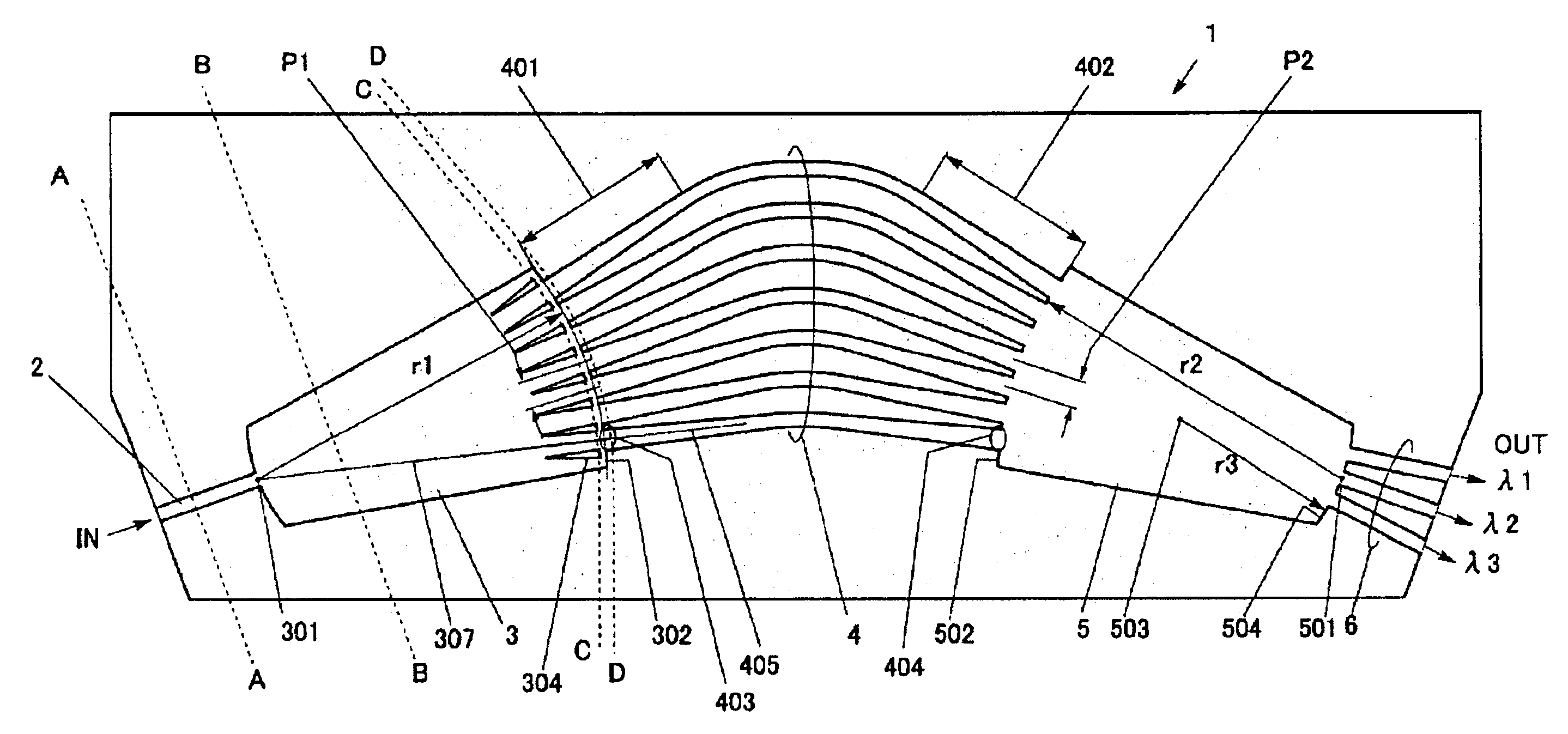
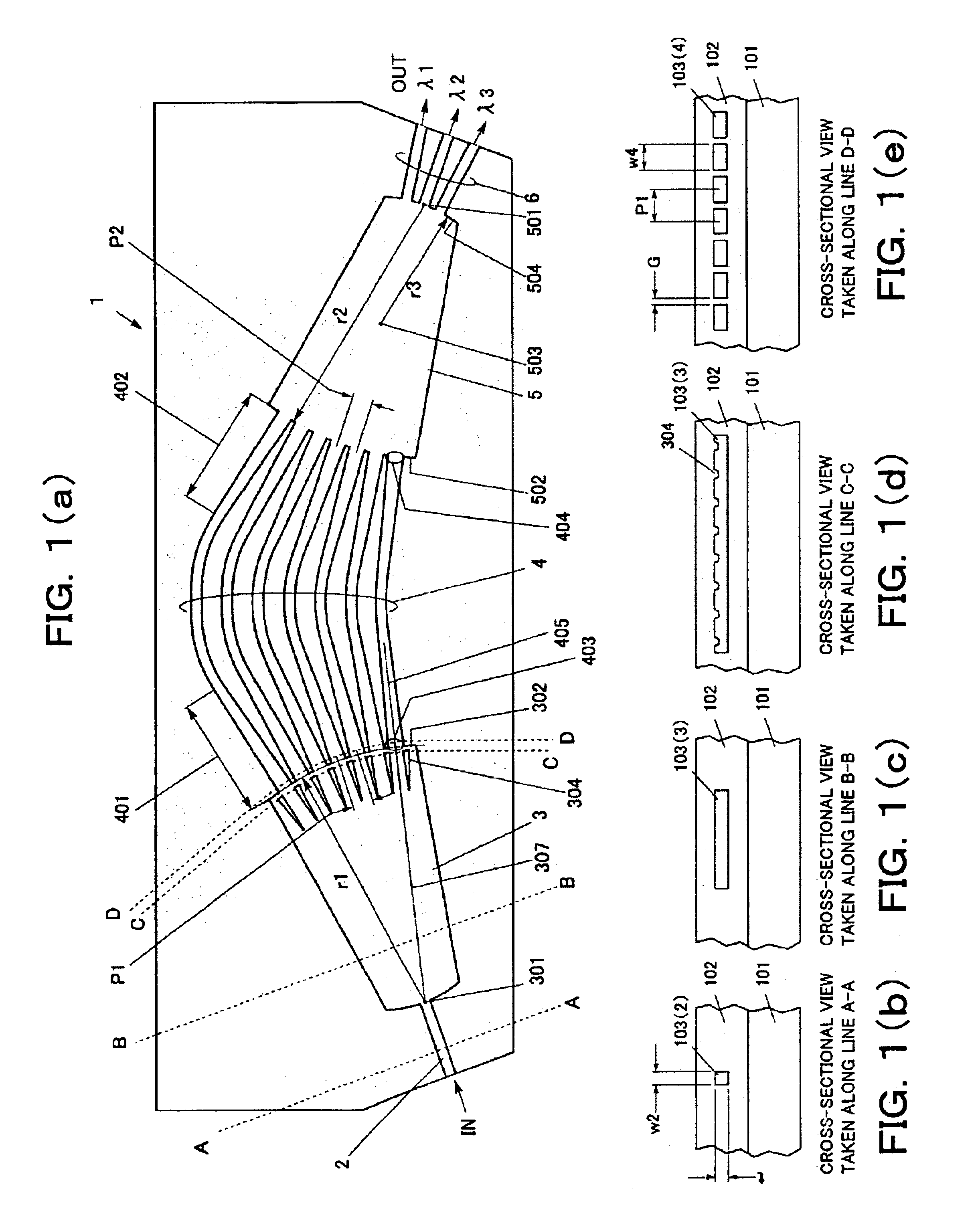
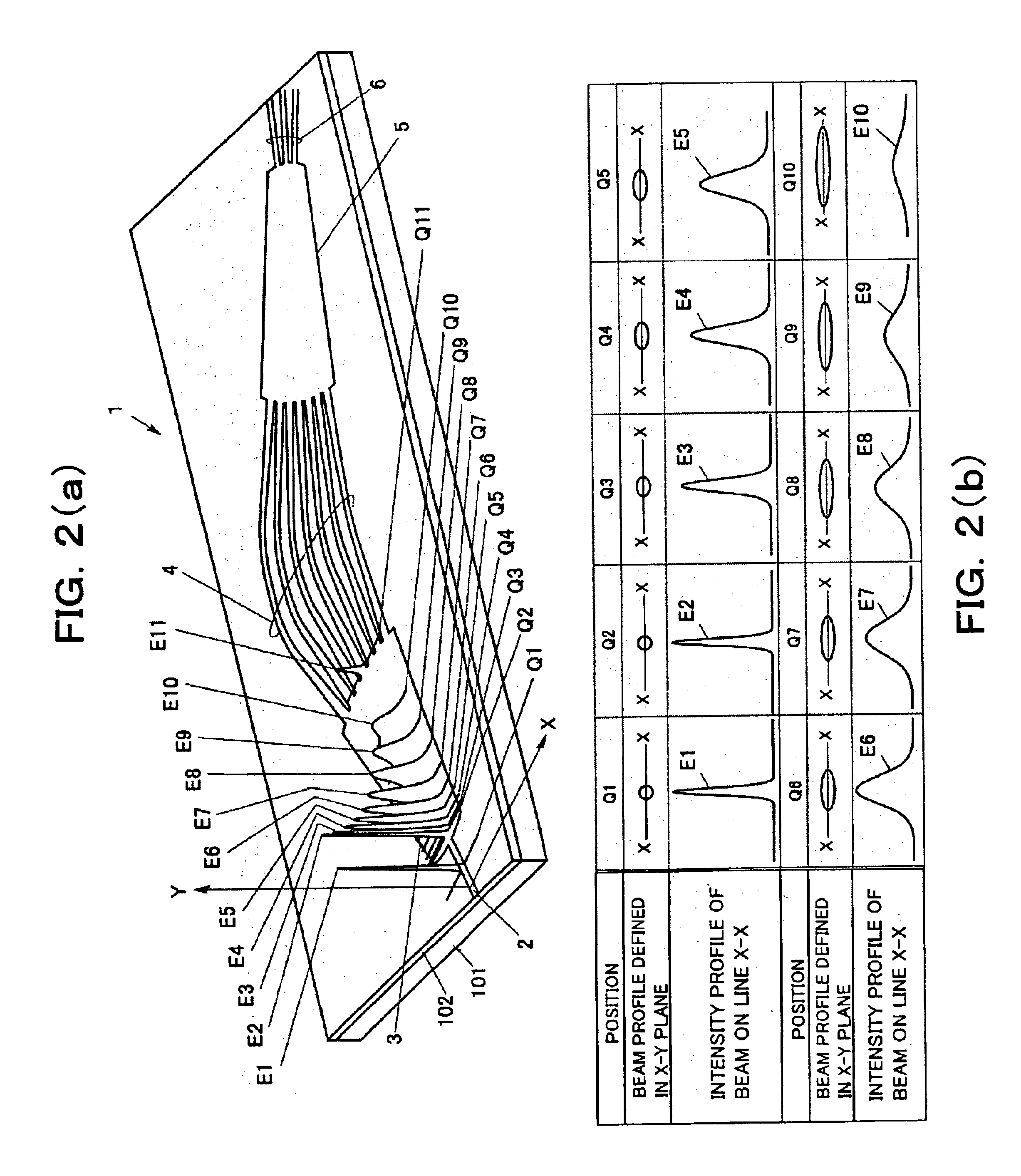
[0100]FIGS. 1(a) to 1(e) are diagrams for explaining a first embodiment of the present invention. FIG. 1(a) is a plan view showing an arrayed waveguide grating type wavelength division multiplexer / demultiplexer according to the first embodiment of the present invention, FIG. 1(b) a cross-sectional view taken along a line A—A in FIG. 1(a), FIG. 1(c) a cross-sectional view taken along a line B—B in FIG. 1(a), FIG. 1(d) a cross-sectional view taken along a line C—C in FIG. 1(a), and FIG. 1(e) a cross-sectional view taken along a line D—D in FIG. 1(a).

[0101]As shown in FIG. 1(a), the arrayed waveguide grating type wavelength division multiplexer / demultiplexer 1 of the present embodiment is also arranged to include an input waveguide 2, an input slab waveguide (hereinafter sometimes simply referred to as “input slab”) 3, a phase-grating waveguide array (hereinafter sometimes simply referred to as ...

second embodiment

[0132](B) Description of Second Embodiment

[0133](B1) Description of Arrangement and Operation

[0134]FIGS. 8(a) to 8(e) are diagrams each for explaining a second embodiment of the present invention. Similarly to FIGS. 1(a) to 1(e), FIG. 8(a) is a plan view showing an AWG type wavelength division multiplexer / demultiplexer according to the second embodiment of the present invention, FIG. 8(b) a cross-sectional view taken along a line A—A in FIG. 8(a), FIG. 8(c) a cross-sectional view taken along a line B—B in FIG. 8(a), FIG. 8(d) a cross-sectional view taken along a line C—C in FIG. 8(a), and FIG. 8(e) a cross-sectional view taken along a line D—D in FIG. 8(a).

[0135]Reference numerals in FIG. 8(a) represent components corresponding to those shown in FIG. 1(a). That is, in FIG. 8, reference numeral 1 represents the AWG type wavelength division multiplexer / demultiplexer, 2 the input waveguide, 3 the input slab, 4 the phase-grating waveguide array, 5 the output slab, and 6 the output waveg...

third embodiment

[0155](C) Description of Third Embodiment

[0156](C1) Description of Arrangement and Operation

[0157]FIGS. 14(a) to 14(e) are diagrams for explaining a second embodiment of the present invention. Similarly to FIGS. 1(a) to 1(e), FIGS. 8(a) to 8(e), FIGS. 12(a) to 12(e), and FIGS. 13(a) to 13(e), FIG. 14(a) is a plan view showing an AWG type wavelength division multiplexer / demultiplexer according to the third embodiment of the present invention, FIG. 14(b) a cross-sectional view taken along a line A—A in FIG. 14(a), FIG. 14(c) a cross-sectional view taken along a line B—B in FIG. 14(a), FIG. 14(d) a cross-sectional view taken along a line C—C in FIG. 14(a), and FIG. 14(e) a cross-sectional view taken along a line D—D in FIG. 14(a).

[0158]Reference numerals are also introduced into FIGS. 14(a) to 14(e) in a similar manner so that they indicate the components corresponding to those in FIGS. 1(a) to 1(e), 8(a) to 8(e), 12(a) to 12(e) and 13(a) to 13(e). That is, reference numeral 1 represen...


PUM


Abstract

In an arrayed waveguide grating type wavelength division demultiplexer including an input waveguide, an input slab waveguide, a phase-grating waveguide array composed of a plurality of optical channel waveguides, an output slab waveguide, and a plurality of output waveguides provided in a core layer so as to form a predetermined pattern, the input slab waveguide is configured to have portions with locally varied thickness in at least the core layer or the cladding layer at the vicinity of each coupling portion of the optical channel waveguide depending on the layout of the optical channel waveguides, whereby the input slab waveguide is made to have a high refractive index region having a refractive index relatively higher than surrounding regions thereof. With this arrangement of the device, the device can be applied to a case where it is undesirable to dope materials of Ge, Ti and Ce. Moreover, with this arrangement of the device, it becomes possible to avoid deterioration with time passage and reduce polarization dependent loss, thereby to improve optical coupling loss.

Description

BACKGROUND OF THE INVENTION[0001](1) Field of the Invention[0002]The present invention relates to a wavelength division demultiplexer for use in a WDM (Wavelength Division Multiplex) communication in which a plurality of optical signal channels having respectively differing wavelengths are subjected to multiplexing so that the resulting optical signal can be transmitted through a single optical fiber and the transmitted optical signal is subjected to a step of dividing (demultiplexing) into separated optical signals having the respectively differing wavelengths. In particular, the present invention relates to an arrayed waveguide grating type wavelength division demultiplexer employing an array of optical waveguides which is comprised of a substrate, a cladding layer provided on the substrate, and a core layer surrounded with the cladding layer and having a refractive index higher than that of the cladding layer.[0003](2) Description of Related Art[0004]FIGS. 20(a) to 20(d) shows an...

Claims


Application Information

Patent Timeline
Patent Type & Authority Patents(United States)
IPC IPC(8): G02B6/10G02B6/34G02B6/12
CPCG02B6/105G02B6/12011G02B6/12014
Inventor TABUCHI, HARUHIKO
Owner FUJITSU LTD
Features
  • R&D
  • Intellectual Property
  • Life Sciences
  • Materials
  • Tech Scout
  • Unparalleled Data Quality
  • Higher Quality Content
  • 60% Fewer Hallucinations
Learn More