Multi-state non-volatile integrated circuit memory systems that employ dielectric storage elements

a dielectric storage element and integrated circuit technology, applied in nanoinformatics, instruments, transistors, etc., can solve the problems of limiting the extent to which a given circuit layout can be shrunk, and the difficulty of performing both of these functions

Inactive Publication Date: 2005-08-02
SANDISK TECH LLC
View PDF122 Cites 260 Cited by
  • Summary
  • Abstract
  • Description
  • Claims
  • Application Information

AI Technical Summary

Benefits of technology

[0017]Two or more electron storage elements can be provided within the storage dielectric of each memory cell that has a gate structure allowing independent control of the electric potential across the substrate surface in respective two or more portions along the length of the memory cell channel. One or two independently programmed and read charge storage regions may be used within each dielectric electron storage element. The enlargement or movement of a region of the dielectric into which electrons are injected, which can occur as the number of erase / programming cycles increases, thus does not affect an adjacent region within the same memory cell. This increases the number of erase / programming cycles that the memory can endure, thus increasing its effective life.
[0019]Further inventive aspects of the Dual Storage Element Cell include providing a third dielectric storage element under the select gate of each memory cell in which a charge storage region is utilized. This allows three bits of data to be stored in each memory cell when each charge storage region is operated in two states (binary operation) but more data is stored in a single cell if some or all of the charge storage regions are operated in more than two states. Additionally, a memory cell array manufacturing process utilizing dielectric spacers in a mask to define widths of control (steering) gate lines may optionally be utilized to reduce one dimension of the memory cells in order to increase the data storage density of the array.
[0021]An improvement in the NAND array eliminates the usual metallurgical source and drain regions in the substrate between adjacent word lines and storage elements along lengths of NAND memory cell strings. Instead, the word lines and charge storage elements are packed closer together in a manner that practically doubles the density of the charge storage elements along the NAND strings. That is, additional word lines and charge storage elements are positioned in the spaces currently occupied by source and drain diffusions in NAND strings of memory cells. This improved array is operated in the same manner as a NAND array with memory cell source and drain regions.

Problems solved by technology

It is often difficult to perform both of these functions in an optimum manner with a single voltage.
But since there are limits of how far a given circuit layout can be shrunk by scaling through simple demagnification, efforts are so directed toward redesigning cells so that one or more features takes up less area.

Method used


Image

  • Multi-state non-volatile integrated circuit memory systems that employ dielectric storage elements
  • Multi-state non-volatile integrated circuit memory systems that employ dielectric storage elements
  • Multi-state non-volatile integrated circuit memory systems that employ dielectric storage elements

Examples


Embodiment Construction

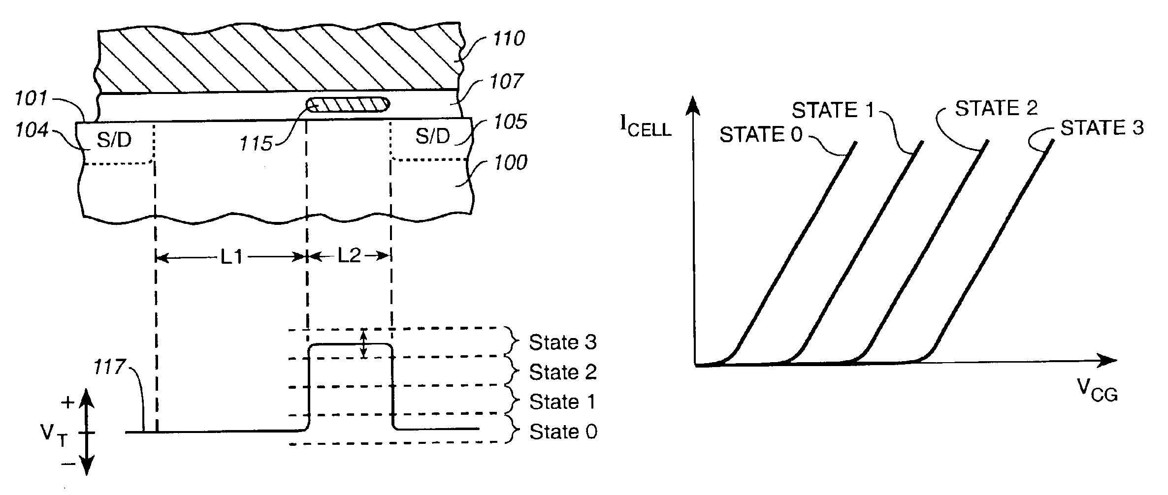
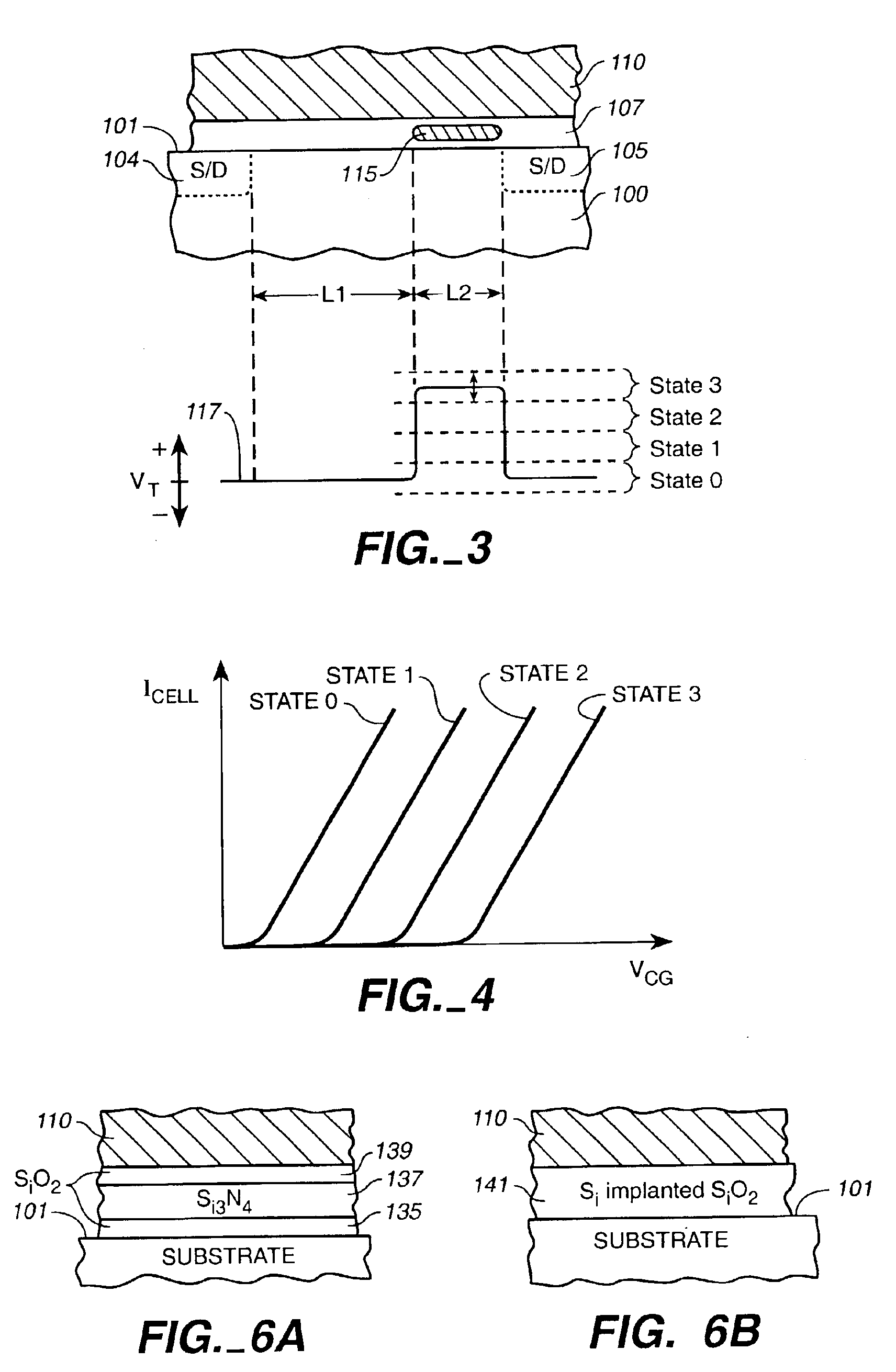
[0050]Several specific memory cell configurations are described with respect to the drawings. In each of them, charge is stored in at least one region of a charge trapping dielectric that is positioned between a conductive gate and the substrate. These memory cell examples may be operated either in a binary mode, where one bit of data is stored in each charge storage region, or in a multi-state mode, where more than one bit of data is stored in each charge storage region.

First Memory Cell Example (FIGS. 1-6)

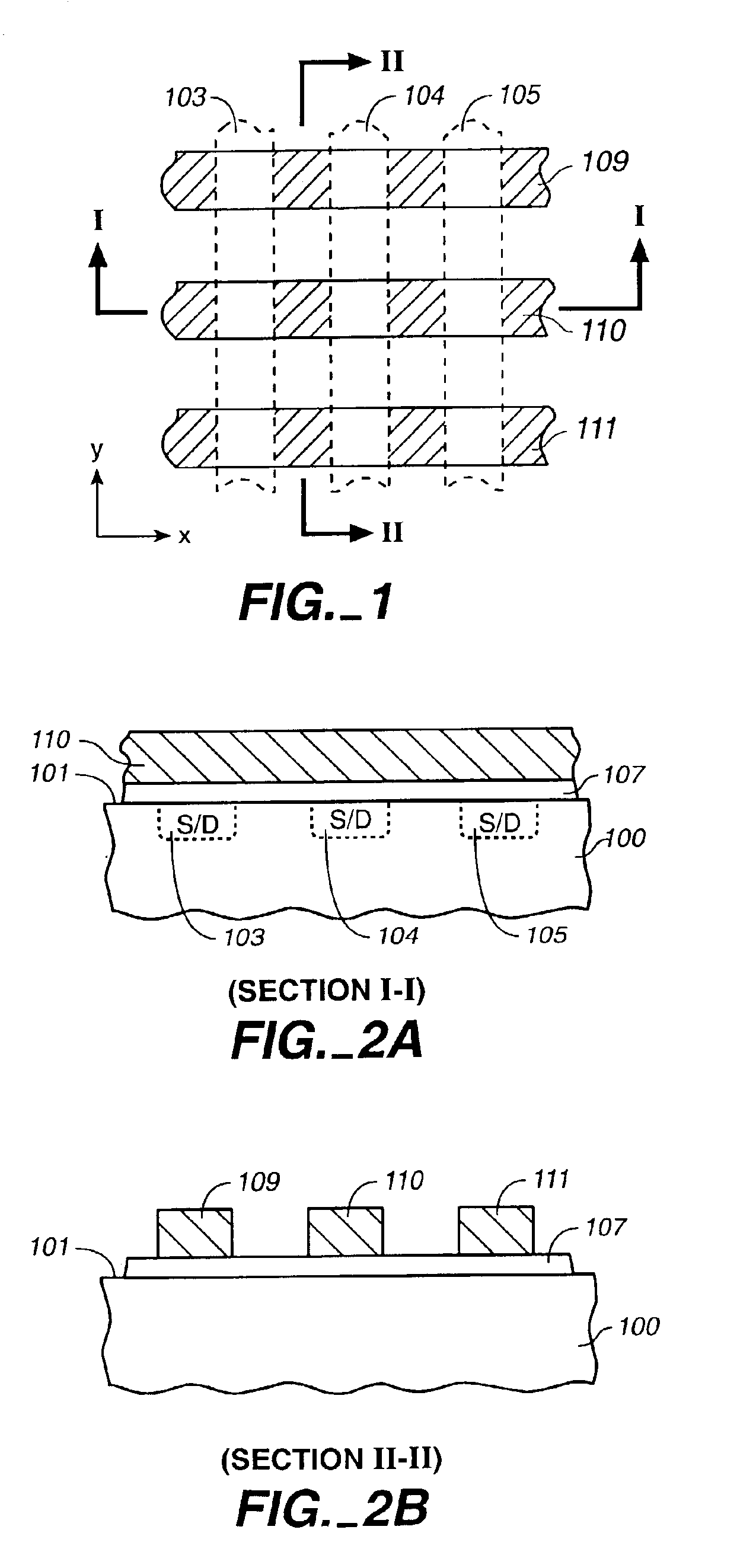
[0051]A few cells of a two-dimensional array of cells is illustrated in FIG. 1 in plan view, with orthogonal sections shown in FIGS. 2A and 2B. Elongated, parallel source and drain diffusions 103, 104 and 105 are formed in a surface 101 of a semi-conductor substrate 100, with their lengths extending in the y-direction and are spaced apart in the x-direction. A dielectric layer 107 including a charge storage material is formed on the substrate surface 101. Elongated, parallel cond...


PUM


Abstract

Non-volatile memory cells store a level of charge corresponding to the data being stored in a dielectric material storage element that is sandwiched between a control gate and the semiconductor substrate surface over channel regions of the memory cells. More than two memory states are provided by one of more than two levels of charge being stored in a common region of the dielectric material. More than one such common region may be included in each cell. In one form, two such regions are provided adjacent source and drain diffusions in a cell that also includes a select transistor positioned between them. In another form, NAND arrays of strings of memory cells store charge in regions of a dielectric layer sandwiched between word lines and the semiconductor substrate.

Description

CROSS REFERENCE TO RELATED APPLICATIONS[0001]This is a continuation-in-part of application Ser. No. 10 / 161,235, filed May 31, 2002, now abandoned, publication No. 2003-0080370-A1, which in turn is a continuation-in-part of application Ser. No. 10 / 002,696, filed Oct. 31, 2001 publication No. 2003-0082871-A1, which applications are incorporated herein in their entirety by this reference.FIELD OF THE INVENTION[0002]This invention relates most specifically to non-volatile flash EEPROM (Electrically Erasable and Programmable Read Only Memory) cell arrays of a type using dielectric material charge storage elements.BACKGROUND[0003]There are many commercially successful non-volatile memory products being used today, particularly in the form of small cards, where the memory cells have conductive floating gates, commonly of doped polysilicon material, on which an electron charge is stored to a level of the data state being stored. A common form of such memory cells has a “split-channel” betwe...

Claims


Application Information

Patent Timeline
Patent Type & Authority Patents(United States)
IPC IPC(8): G11C11/56H01L21/70H01L27/115H01L29/66H01L21/8246H01L21/8247H01L29/792G11C16/04H01L29/788
CPCB82Y10/00G11C11/5671G11C16/0466G11C16/0483H01L27/115H01L27/11521H01L27/11524H01L27/11568H01L29/4234H01L29/7923G11C16/0475G11C16/0491G11C2216/06Y10S438/947H10B41/35H10B43/30H10B69/00H10B41/30
Inventor HARARI, ELIYAHOUSAMACHISA, GEORGEYUAN, JACK H.GUTERMAN, DANIEL C.
Owner SANDISK TECH LLC
Why Eureka
Try Eureka