Vertically integrated photosensor for CMOS imagers

a photosensor and vertical integration technology, applied in the field of semiconductor and imaging devices, can solve the problems of obstructing the use of band gap engineering as an effective design tool, affecting the efficiency of optical and optoelectronic design of the photosensor, and increasing the density of noise current, so as to achieve the effect of high density of interconnection

Inactive Publication Date: 2005-08-09
GOOGLE TECHNOLOGY HOLDINGS LLC
View PDF7 Cites 114 Cited by
  • Summary
  • Abstract
  • Description
  • Claims
  • Application Information

AI Technical Summary

Problems solved by technology

Because the photodiodes (PDs) of CMOS imagers are usually fabricated within the same material layer and with similar processes as the electronics, and these materials and processes are often dominated by and optimized for electronic circuitry, the optical and optoelectronic design of the photosensor are generally compromised.
Representative limitations involve the Si material itself wherein a fixed band gap generally obstructs the use of band gap engineering as an effective design tool.
Moreover, as the photodetector active area is reduced, the dark current becomes dominated by the perimeter causing inter alia the noise current density to increase.
Together, these effects generally operate to degrade the signal to noise performance of the sensor.
This desire for increased signal processing functionality within the pixel escalates competition for ‘real estate’ within the pixel area creating additional problems generally associated with shrinking the PD active area, reducing the fill factor within the pixel, and applying advanced process technologies.
Migration to advanced process technologies may further compromise PD device design and performance.
0.25μ technologies and beyond typically employ silicides that are optically opaque and potentially leaky, as well as shallow trench isolation (STI) which may often lead to higher perimeter-generated dark current levels.
Reduced supply voltages also may negatively impact charge collection and storage capability of the PD.
Moreover, an ever-increasing number of interconnect levels and corresponding isolating dielectric layers generally decreases the optical throughput and coupling efficiency to the photodetector and introduces additional sources of reflection and scattering that can lead to elevated levels of optical crosstalk.
Efforts to improve the level of PD performance can limit flexibility and performance in the CMOS electronics as well.
Minimizing the number of interconnect levels to improve the optical coupling to the PD, for example, may make interconnect routing more difficult and less area-efficient.
The co-integration of the photosensor with the CMOS electronics (i.e., within the same material layer, using the same processes, etc.) within the pixel of CMOS imagers may severely limit both the performance of the photosensor and the flexibility of the system architectural design.
This problem may be further complicated by progression to more advanced CMOS technology generations which generally utilize trench isolation, non-transparent suicides, and increasing numbers of interconnect levels.
The current trend toward increase functionality within the pixel (as with digital pixel sensors—DPS) adds more electronic circuitry within the pixel creating competition for pixel area, decreasing fill factor and further compromising of performance.

Method used


Image

  • Vertically integrated photosensor for CMOS imagers
  • Vertically integrated photosensor for CMOS imagers
  • Vertically integrated photosensor for CMOS imagers

Examples


Embodiment Construction

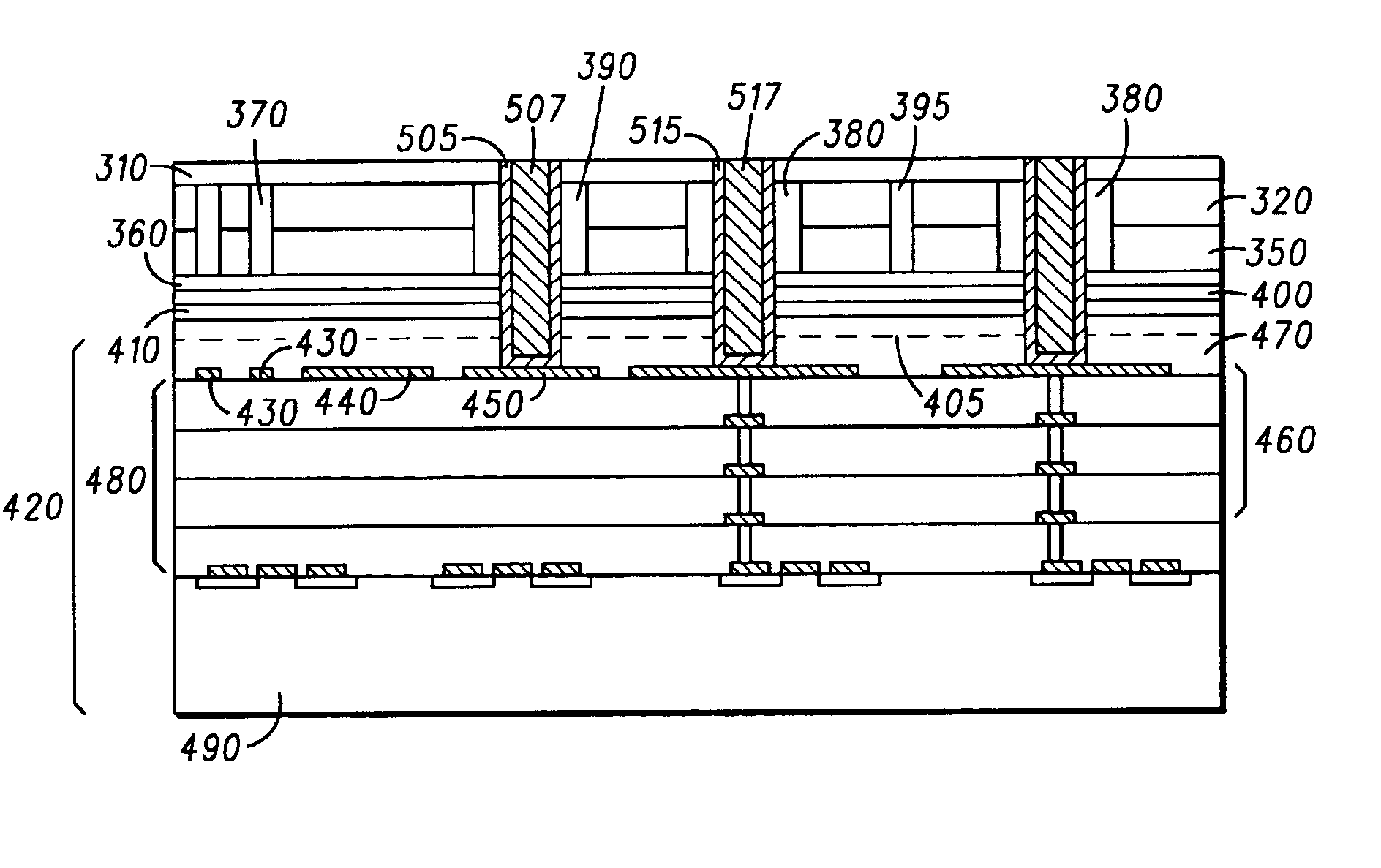
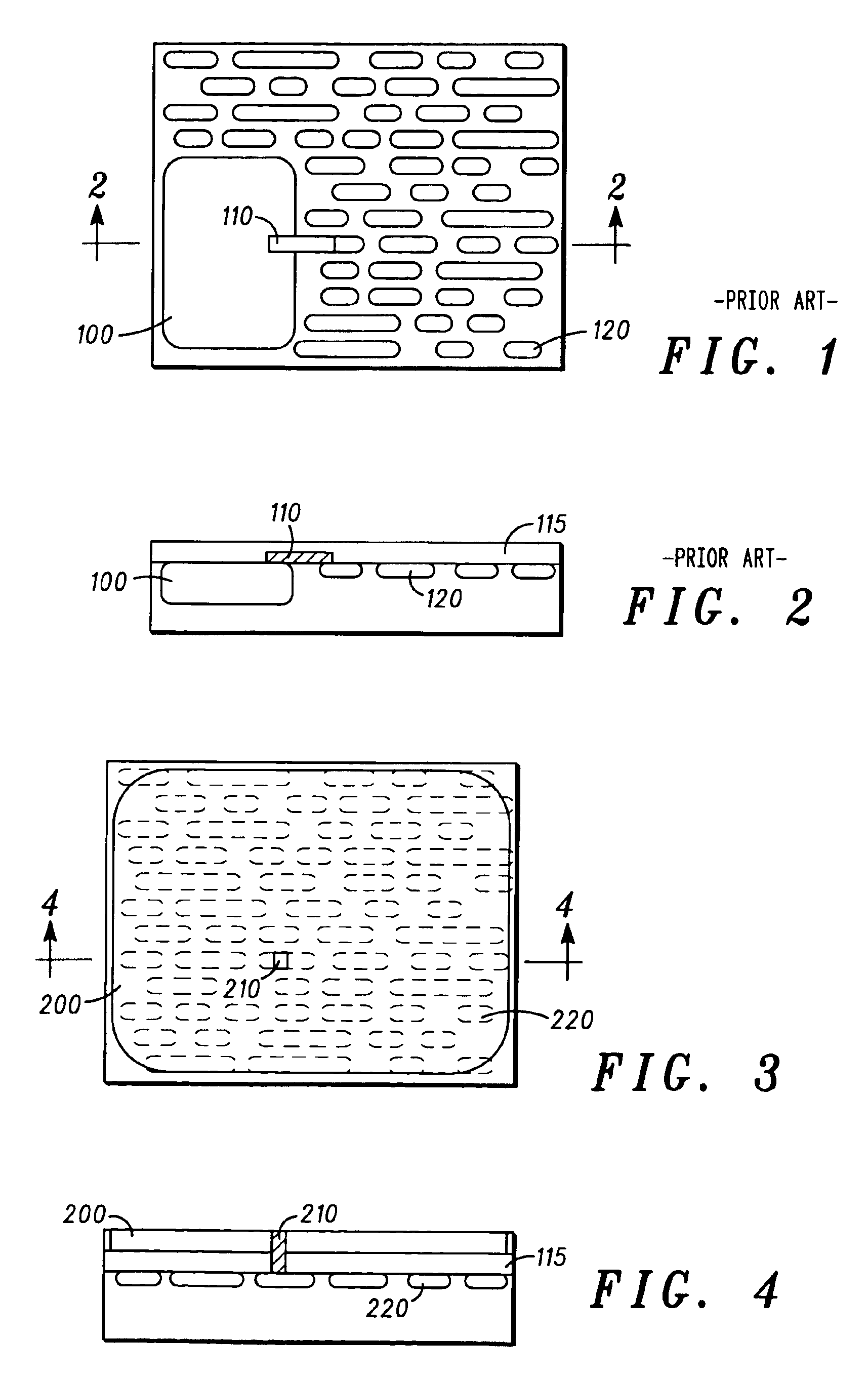
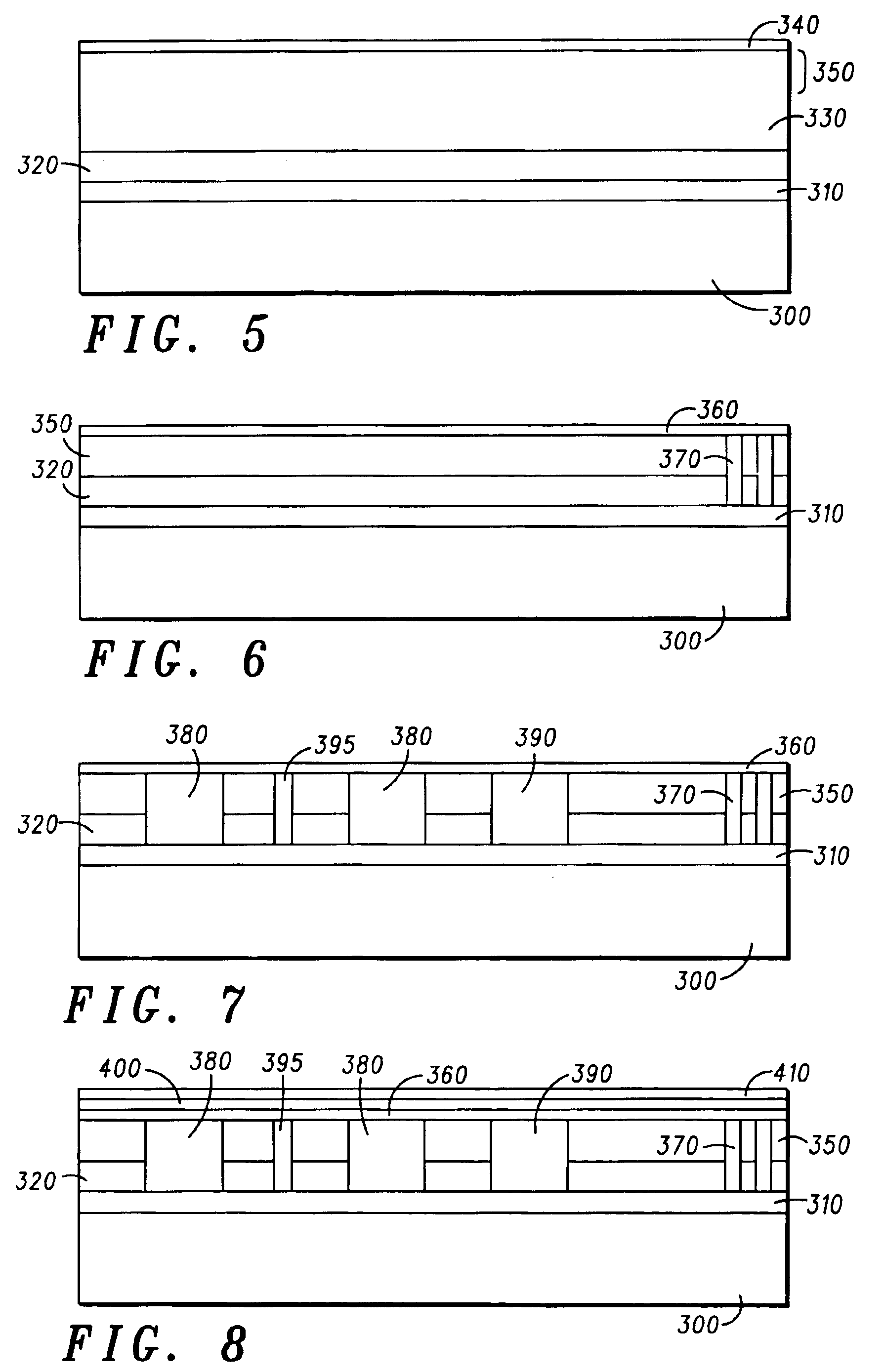
[0029]The following descriptions are of exemplary embodiments of the invention and the inventors' conceptions of the best mode and are not intended to limit the scope, applicability or configuration of the invention in any way. Rather, the following Description is intended to provide convenient illustrations for implementing various embodiments of the invention. As will become apparent, changes may be made in the function and / or arrangement of any of the elements described in the disclosed exemplary embodiments without departing from the spirit and scope of the invention.

[0030]A detailed description of an exemplary application, namely a system and method for providing a vertically integrated photosensing device suitably adapted for use in CMOS imaging applications is presented as a specific enabling disclosure that may be readily generalized by skilled artisans to any application of the disclosed system and method in accordance with various embodiments of the present invention.

[0031...


PUM


Abstract

An exemplary system and method for providing a vertically integrated photosensing element suitably adapted for use in CMOS imaging applications is disclosed as comprising inter alia: a processed CMOS layer (420); and a photosensing element (380) fabricated in a vertically integrated optically active layer (320, 350), where the optically active layer (320, 350) is bonded to the CMOS layer (420) and the optically active layer (320, 350) is positioned near a metalization surface (405) of the CMOS layer (420). Disclosed features and specifications may be variously controlled, configured, adapted or otherwise optionally modified to further improve or otherwise optimize photosensing performance or other material characteristics. Exemplary embodiments of the present invention representatively provide for integrated photosensing components that may be readily incorporated with existing technologies for the improvement of CMOS imaging, device package form factors, weights and / or other manufacturing, device or material performance metrics.

Description

FIELD OF INVENTION[0001]The present invention generally relates to semiconductor and imaging devices; and more particularly, to systems and methods for vertically integrating photosensing elements for use in CMOS imaging applications.BACKGROUND[0002]CMOS imagers have begun to challenge CCDs in many electronic imaging applications and are gaining in popularity. The primary advantages of CMOS imagers are their relatively low cost generally resulting from the use of standard, high-volume CMOS processes and their ability to be integrated with native CMOS electronics for control and image processing; this in contrast to CCDs, which typically employ specialized processing optimized for image capturing operations that are not generally amenable to large-scale integration of electronics.[0003]Because the photodiodes (PDs) of CMOS imagers are usually fabricated within the same material layer and with similar processes as the electronics, and these materials and processes are often dominated ...

Claims


Application Information

Patent Timeline
Patent Type & Authority Patents(United States)
IPC IPC(8): H01L31/062H01L31/06H01L27/146
CPCH01L27/1463H01L27/14636H01L27/14643
Inventor HOLM, PAIGE M.CANDELARIA, JON J.
Owner GOOGLE TECHNOLOGY HOLDINGS LLC
Why Eureka
Try Eureka