Pixel clock generating device, laser scanning device, and image forming device

a pixel clock and laser scanning technology, applied in the direction of electrographic process equipment, instruments, printing, etc., can solve the problems of different scanning lengths of individual lasers, non-uniform scanning speed of laser beams, image degradation,

Inactive Publication Date: 2005-08-09
RICOH KK
View PDF15 Cites 52 Cited by
  • Summary
  • Abstract
  • Description
  • Claims
  • Application Information

AI Technical Summary

Benefits of technology

[0055]According to the above invention, it becomes possible to provide an image forming device including the above laser scanning device.

Problems solved by technology

However, the distance between one reflection plane and the rotational axis of the deflector may change, as a result, there arises non-uniformity of the scanning speed of the laser beam (that is, the speed of the light spot moving on the medium during scanning), and causes image degradation.
This causes different scanning lengths of individual lasers and therefore image degradation.
In the above related art involving changing the frequency of the pixel clock (it is the so-called “Frequency Modulation”), however, the configuration of the control unit for the pixel clock becomes complicated, and becomes more complicated if the frequency modulation width becomes smaller.
Therefore, this technique is not suitable to delicate control.
Thus, it is difficult to eliminate the scanning non-uniformity even when the same reflection plane of the deflector is used to reflect the laser beam, because there is a limitation to the precision of controlling the rotational motor of the deflector.

Method used


Image

  • Pixel clock generating device, laser scanning device, and image forming device
  • Pixel clock generating device, laser scanning device, and image forming device
  • Pixel clock generating device, laser scanning device, and image forming device

Examples


first embodiment

[0091]The First Embodiment

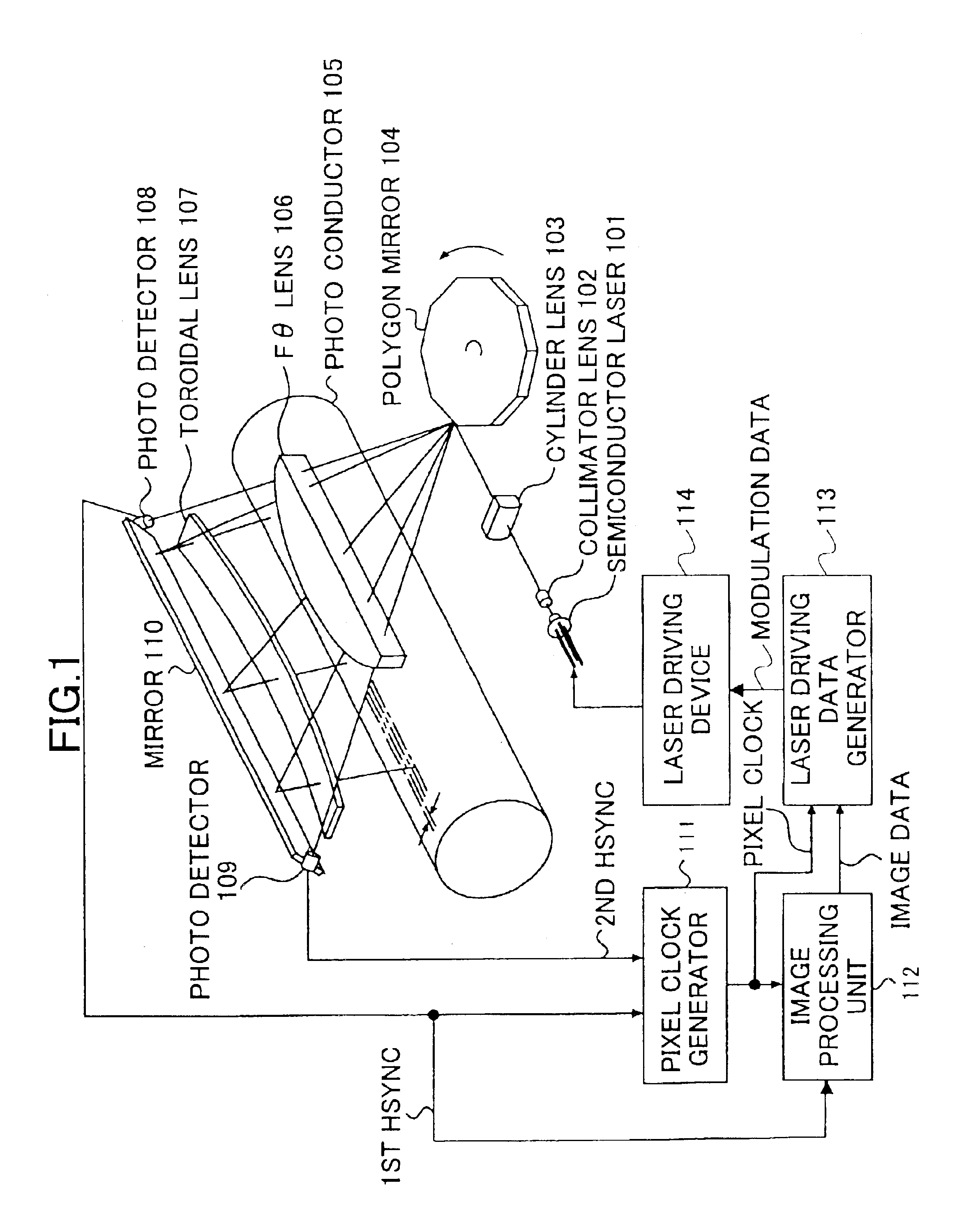
[0092]FIG. 1 is a view of a configuration of an image forming device according to a first embodiment of the present invention.

[0093]Referring to FIG. 1, the image forming device 100 comprises a semiconductor laser 101 that is driven by a laser driving device 114 to emit a laser beam having any time spread. The laser beam from the semiconductor laser 101 is shaped by a collimator 102 and a cylinder lens 103, and is emitted to a polygon mirror 104 that is a prism having a regular polygonal base and has a rotational axis perpendicularly passing through the center of the base, and is reflected to scan the photo conductor 105 periodically. Before the reflected laser beam is applied to the photo conductor 105, its optical axis is bent after passing an fθ lens 106, a mirror 110 and a toroidal lens 107.

[0094]The laser beam is reflected to the photo conductor 105 and forms a light spot, thereby forming an electrostatic latent image on the photo conductor 101 in resp...

second embodiment

[0157]The Second Embodiment

[0158]Below, the second embodiment of the present invention will be explained with reference to the figures.

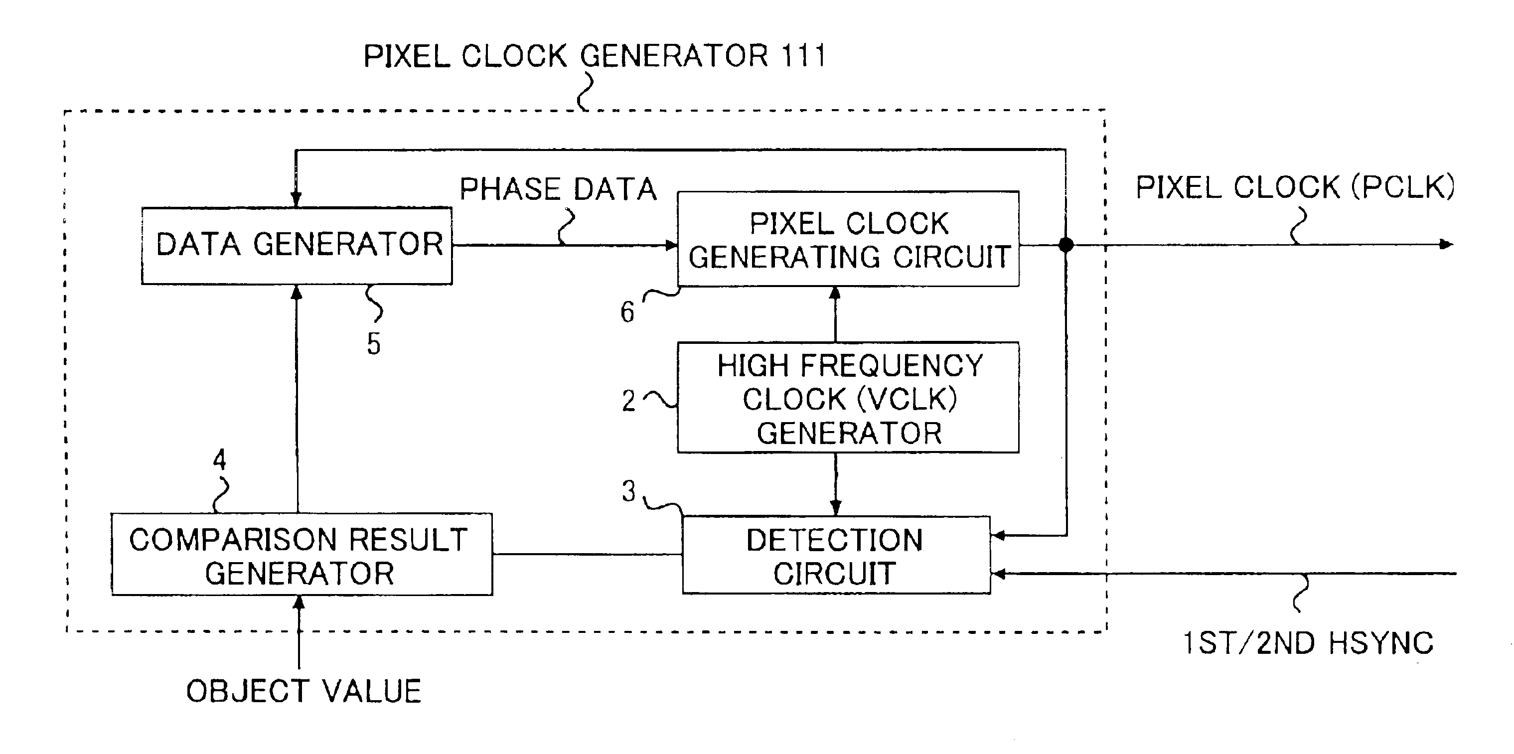
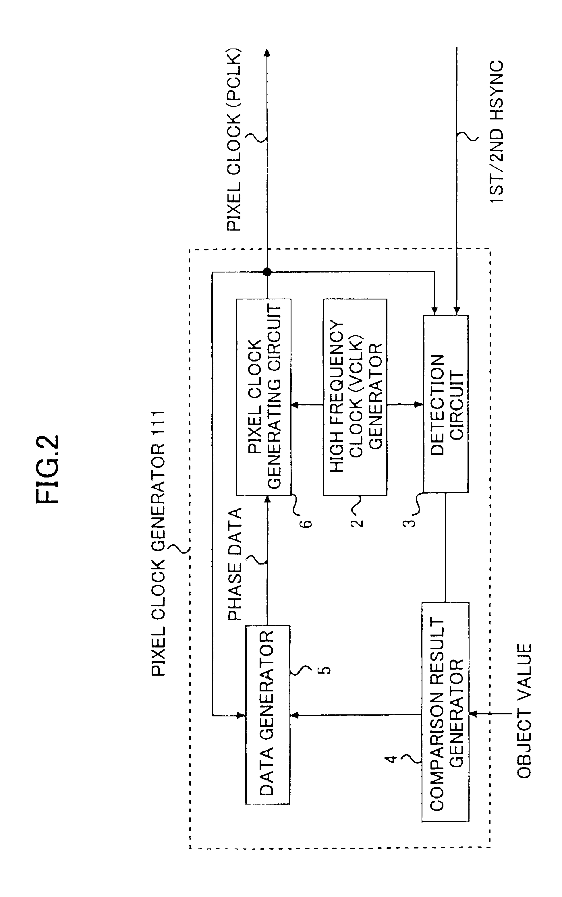
[0159]FIG. 13 is a block diagram showing a configuration of a pixel clock generator 211 according to the second embodiment of the present invention.

[0160]Differing from the pixel clock generator 111 in the first embodiment, the pixel clock generator 211 has a pixel clock generating circuit 15 replacing the pixel clock generating circuit 6 in the pixel clock generator 111. The pixel clock generating circuit 15 receives input of the first and the second horizontal synchronization signals. By such a configuration, it is able to generate a pixel clock with its phase synchronized, and make the write positions in different lines uniform.

[0161]FIG. 14 is a block diagram showing a configuration of the pixel clock generating circuit 15;

[0162]Referring to FIG. 14, differing from the pixel clock generating circuit 15 in the first embodiment, a counter 34 and a ...

third embodiment

[0169]The Third Embodiment

[0170]In the first embodiment, the explanation is made of a case in which the image forming device 100 utilizes a single beam optical system (a single beam scanning device), but it is possible to replace the single beam scanning device by a multi-beam scanning device. Below, as the third embodiment of the present invention, an image forming device utilizing a multi-beam beam scanning device will be explained with reference to the figures.

[0171]FIG. 16 is a perspective view of a configuration of a multi-beam scanning device 300 incorporated into an image forming device according to a second embodiment of the present invention. As shown in FIG. 16, the multi-beam scanning device 300 has a semiconductor laser array 301 (corresponding to the semiconductor laser arrays 301a and 301b in FIG. 16). As shown in FIG. 17, each semiconductor laser array 301a or 301b includes two light emission sources 302a and 302b which are separated at a distance of ds=25 μm, and arr...


PUM


Abstract

A pixel clock generating device includes a measurement unit that measures a scanning time required for scanning a length and outputs a measured value, a pixel clock generating unit that generates a pixel clock, and a reference clock generating unit that generates a reference clock having a frequency higher than the pixel clock. A phase of the pixel clock is controlled based on (i) the reference clock and (ii) a comparison result between the measured scanning time and a preset scanning time.

Description

BACKGROUND OF THE INVENTION[0001]1. Field of the Invention[0002]The present invention relates to a pixel clock generating device, a laser scanning device, and an image forming device.[0003]2. Description of the Related Art[0004]FIG. 25 shows a general configuration of an image forming device such as a laser printer, or a digital copy machine. As shown in FIG. 25, a laser beam emitted from a semiconductor laser unit 1009 is scanned by a rotational polygon mirror 1003, and is reflected to a photo conductor 1001 that functions as an object medium. The light spot of the laser beam on the photo conductor 1001 forms an electrostatic latent image there. Once the polygon mirror 1003 finishes the scanning of one line, it deflects the laser beam to irradiate a photo detector 1004. The photo detector 1004 converts the irradiated laser beam into electrical signals and inputs the signals to a PLL (Phase Locked Loop) circuit 1006. The PLL circuit generates a clock signal (called “pixel clock” or ...

Claims


Application Information

Patent Timeline
Patent Type & Authority Patents(United States)
IPC IPC(8): G02B26/12H04N1/047H04N1/053H04N1/113H04N1/12B41J2/44G02B26/10G03G15/04H04N1/036
CPCG02B26/127H04N1/053H04N1/1135H04N1/12H04N2201/0471H04N2201/04768H04N2201/04732H04N2201/04744H04N2201/02439H04N2201/04794
Inventor OZASA, DANISHIDA, MASAAKINIHEI, YASUHIROOMORI, ATSUFUMI
Owner RICOH KK
Why Eureka
Try Eureka