Hydrogen assisted undoped silicon oxide deposition process for HDP-CVD

Inactive Publication Date: 2005-08-16
APPLIED MATERIALS INC
View PDF126 Cites 279 Cited by
  • Summary
  • Abstract
  • Description
  • Claims
  • Application Information

AI Technical Summary

Benefits of technology

[0007]Embodiments of the present invention pertain to an improved method of depositing silicon oxide films using HDP-CVD deposition techniques. These embodiments enable improved gap-fill capabilities as compared to HDP-C

Problems solved by technology

Smaller feature sizes have resulted in the presence of increased aspect ratio gaps for some applications, for example, b

Method used


Image

  • Hydrogen assisted undoped silicon oxide deposition process for HDP-CVD
  • Hydrogen assisted undoped silicon oxide deposition process for HDP-CVD
  • Hydrogen assisted undoped silicon oxide deposition process for HDP-CVD

Examples


Example

I. Introduction

[0020]Embodiments of the present invention deposit an improved silicon oxide layer using high density plasma CVD techniques. The deposited layer has improved gap-fill capabilities as compared to some prior art silicon oxide deposition techniques. Films deposited by the method of the present invention are suitable for use in the fabrication of integrated circuits having feature sizes of 0.18 microns or less.

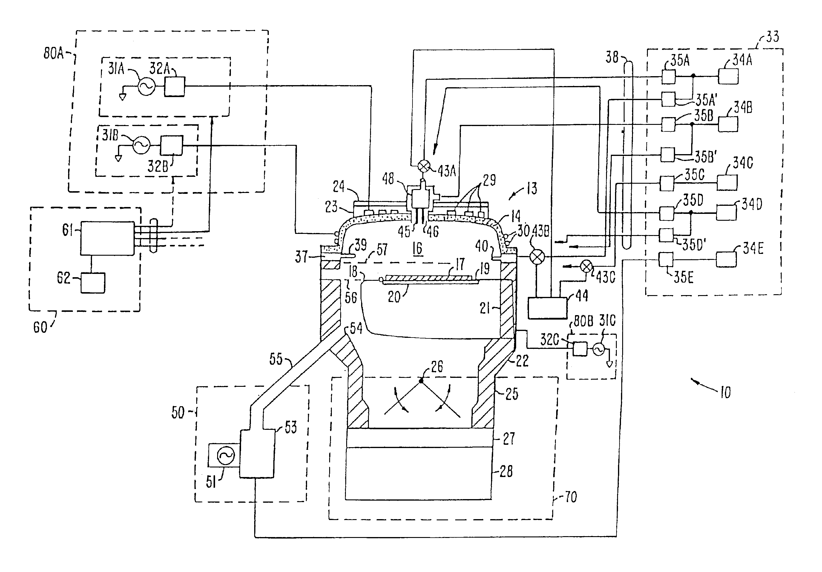
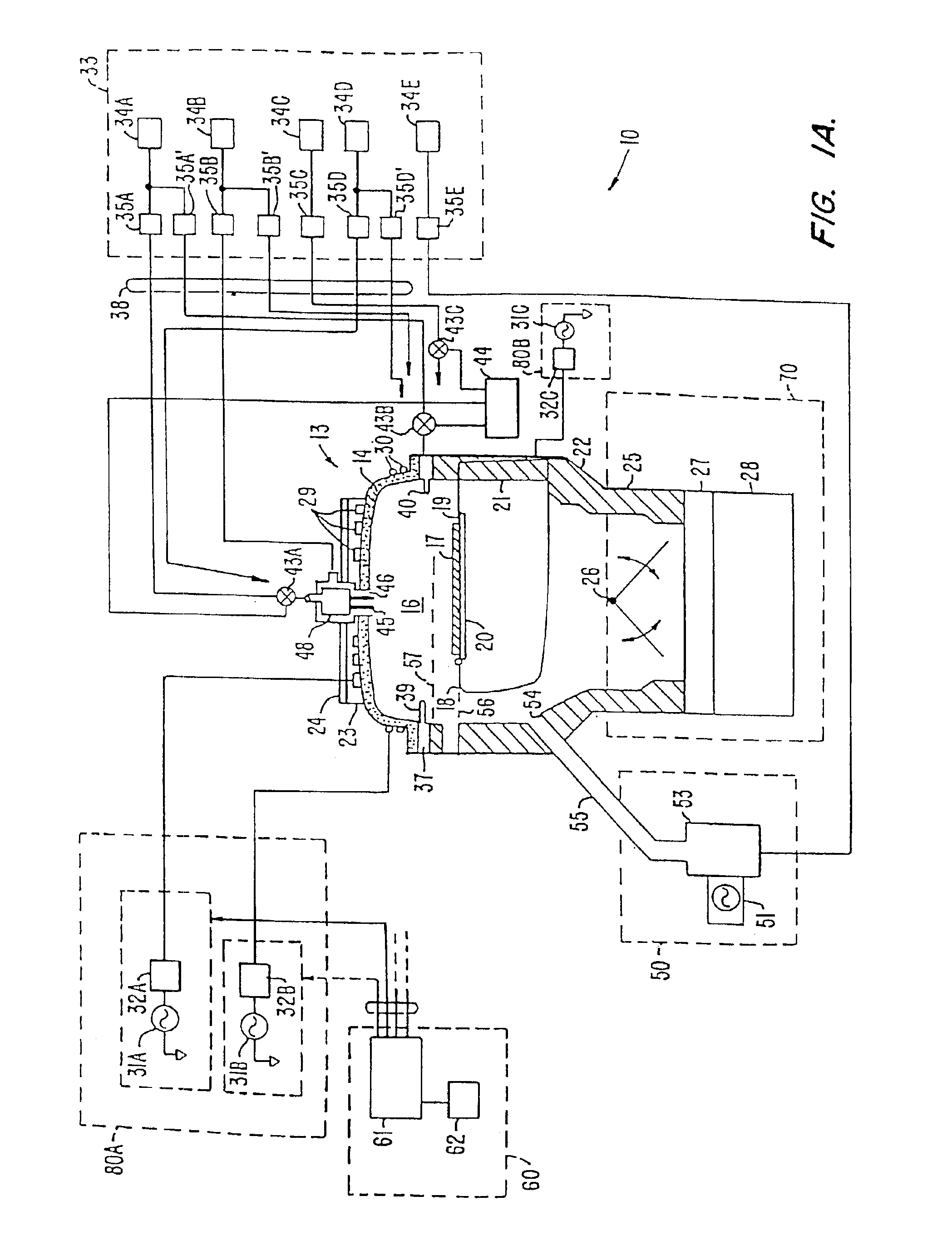
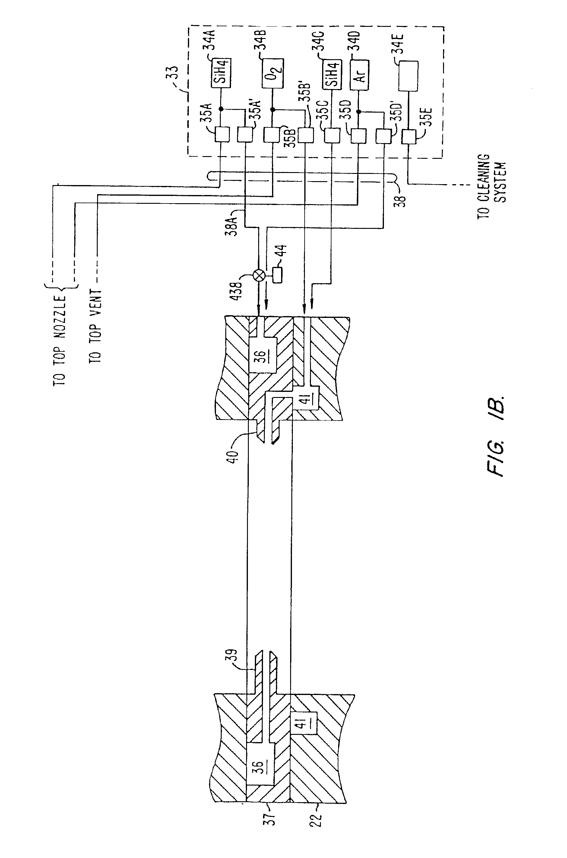
[0021]Embodiments of the present invention can be implemented using a variety of high density plasma CVD substrate processing chambers including chambers in which a plasma is formed by the application of RF energy to a coil that at least partially surrounds a portion of the chamber and chambers that use ECR plasma formation techniques. An example of an inductively-coupled HDP-CVD chamber in which embodiments of the method of the present invention can be practiced is set forth below.

II. Exemplary Substrate Processing System

[0022]FIG. 1A illustrates one embodiment of ...


PUM

PropertyMeasurementUnit
Temperatureaaaaaaaaaa
Percent by atomaaaaaaaaaa
Temperatureaaaaaaaaaa

Abstract

A substrate processing apparatus comprising a substrate processing chamber, a gas distribution system operatively coupled to the chamber, a high density plasma power source, a controller operatively coupled to the gas distribution system and the high density plasma power source and a memory coupled to the controller. The memory includes computer instructions embodied in a computer-readable format. The computer instructions comprise (i) instructions that control the gas distribution system to flow a process gas comprising a silane gas, an oxygen-containing source, an inert gas and a hydrogen-containing source that is either molecular hydrogen or a hydride gas that does not include silicon, boron or phosphorus and (ii) instructions that control the high density plasma source to form a plasma having an ion density of at least 1×10¹¹ ions/cm3 from the process gas to deposit the silicon oxide layer over the substrate.

Description

CROSS-REFERENCES TO RELATED APPLICATIONS[0001]This application is a division of U.S. application Ser. No. 09 / 854,406, filed May 11, 2001, now U.S. Pat. No. 6,596,653, entitled “Hydrogen Assisted Undoped Silicon Oxide Deposition Process For HDP-CVD,” having Zhengquan Tan, Dongqing Li, Walter Zygmunt and Tetsuya Ishikawa listed as coinventors. The Ser. No. 09 / 854,406 application is assigned to Applied Materials, Inc., the assignee of the present invention and is hereby incorporated by reference.BACKGROUND OF THE INVENTION[0002]The present invention relates to the manufacture of integrated circuits. More specifically, the invention relates to an improved method of depositing silicon oxide layers for use as insulation layers in such integrated circuits.[0003]One of the primary steps in the fabrication of modern semiconductor devices is the formation of a film, such as a silicon oxide, on a semiconductor substrate. Silicon oxide is widely used as an insulating layer in the manufacture of...

Claims


Application Information

Patent Timeline
IPC IPC(8): C23C16/40H01L21/70H01L21/02H01L21/762H01L21/768H01L21/316
CPCC23C16/401H01L21/02164H01L21/02211H01L21/02274H01L21/31612H01L21/76229H01L21/76837
Inventor TAN, ZHENGQUANLI, DONGQINGZYGMUNT, WALTERISHIKAWA, TETSUYA
Owner APPLIED MATERIALS INC
Why Eureka
Try Eureka