Optical recording medium, method for manufacturing the same and target used for sputtering process

a technology of optical recording medium and manufacturing method, which is applied in the direction of instruments, photomechanical equipment, thermography, etc., can solve the problems of difficult to improve long-time storage reliability, data recorded in write-once type optical recording medium cannot be erased and rewritten, and achieve the effect of reducing the load on the global environmen

Inactive Publication Date: 2005-08-16
TDK CORPARATION +1
View PDF9 Cites 42 Cited by
  • Summary
  • Abstract
  • Description
  • Claims
  • Application Information

AI Technical Summary

Benefits of technology

[0010]It is another object of the present invention to provide a method for manufacturing an optical recording medium including a recording layer formed of materials which place minimal load on the global environment.
[0011]It is a further object of the present invention is to provide a target used for a sputtering process, which can form a recording layer of an optical recording medium of materials which place minimal load on the global environment.
[0013]According to the present invention, since each of Fe, Al and Si is one of the most commonplace elements on earth and places only an extremely light load on the global environment, an optical recording medium including a recording layer containing as a primary component an alloy containing such elements can greatly lower the load placed on the global environment.
[0015]The inventors did a study that will be explained with reference to the ternary composition diagram shown in FIG. 1. In this ternary composition diagram, x1, y1 and z1 represent the atomic ratios (atomic %) of Fe, Al and Si in the composition of the alloy contained in the at least one recording layer of the optical recording medium as a primary component. The inventors discovered that when each of x1, y1 and z1 of the alloy composition [x1, y1 and z1] in terms of the ternary composition diagram fell within the region of the pentagon defined by straight lines connecting a point A [57, 43, 0], a point B [0, 55, 45], a point C [15, 0, 85], a point D [89, 11, 0] and a point E [0, 16, 84] in the ternary composition diagram, it was possible to reproduce a signal having a high C / N ratio and low jitter, effectively suppress cross-talk of data and improve the recording sensitivity of the optical recording medium.
[0019]According to this preferred aspect of the present invention, since the at least one recording layer is physically and chemically protected by the dielectric layer, degradation of recorded data can be effectively prevented over a long period.
[0023]According to the present invention, it is possible to fabricate an optical recording medium which can reproduce a signal having a high C / N ratio and low jitter, can effectively suppress cross-talk of data and has an improved recording sensitivity.

Problems solved by technology

Unlike data recorded in a data rewritable type optical recording medium, data recorded in a write-once type optical recording medium cannot be erased and rewritten.
However, since an organic dye is degraded when exposed to sunlight or the like, it is difficult to improve long-time storage reliability in the case where an organic dye is used as the material of the recording layer.
However, the inorganic materials for forming recording layers of the optical recording medium disclosed in Japanese Patent Application Laid Open No. 62-204442 include materials which place a heavy load on the environment so that the optical recording medium disclosed in Japanese Patent Application Laid Open No. 62-204442 does not satisfy the requirement for protecting global atmosphere.

Method used


Image

  • Optical recording medium, method for manufacturing the same and target used for sputtering process
  • Optical recording medium, method for manufacturing the same and target used for sputtering process
  • Optical recording medium, method for manufacturing the same and target used for sputtering process

Examples


working example 1

[0135]An optical recording medium sample #1-1 was fabricated in the following manner.

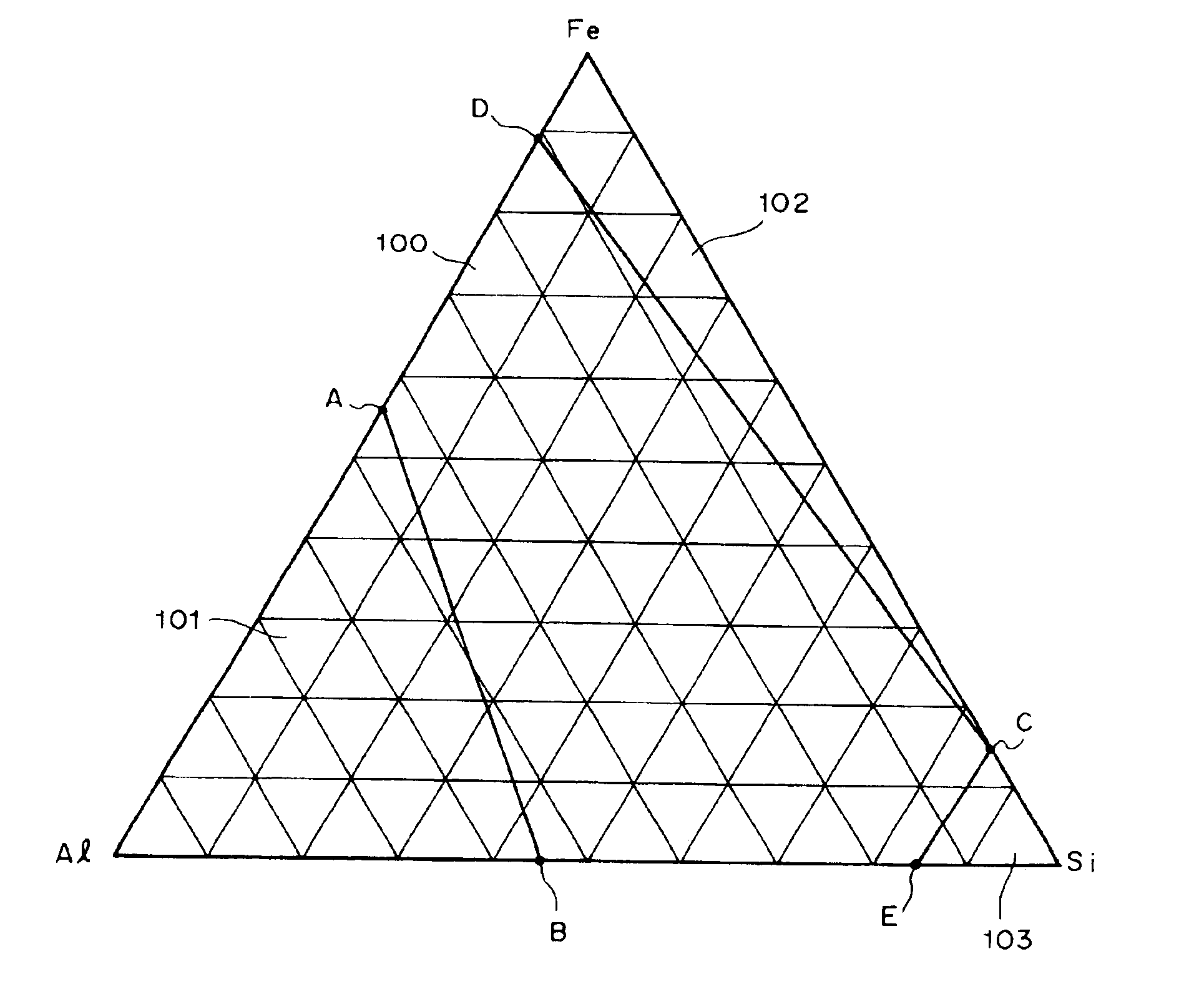
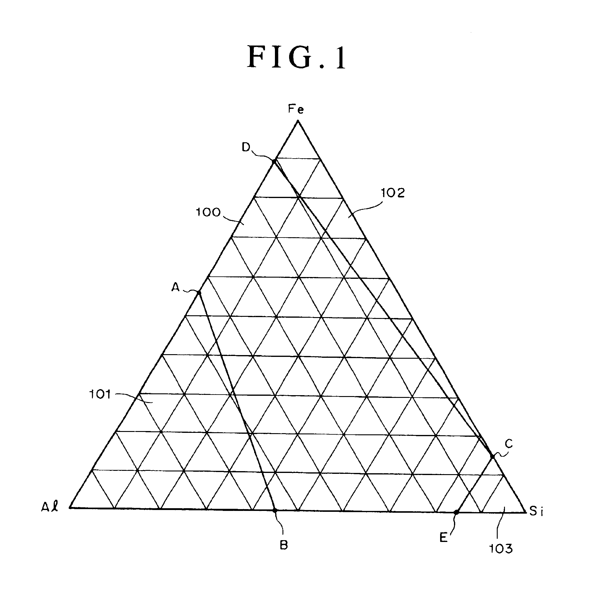
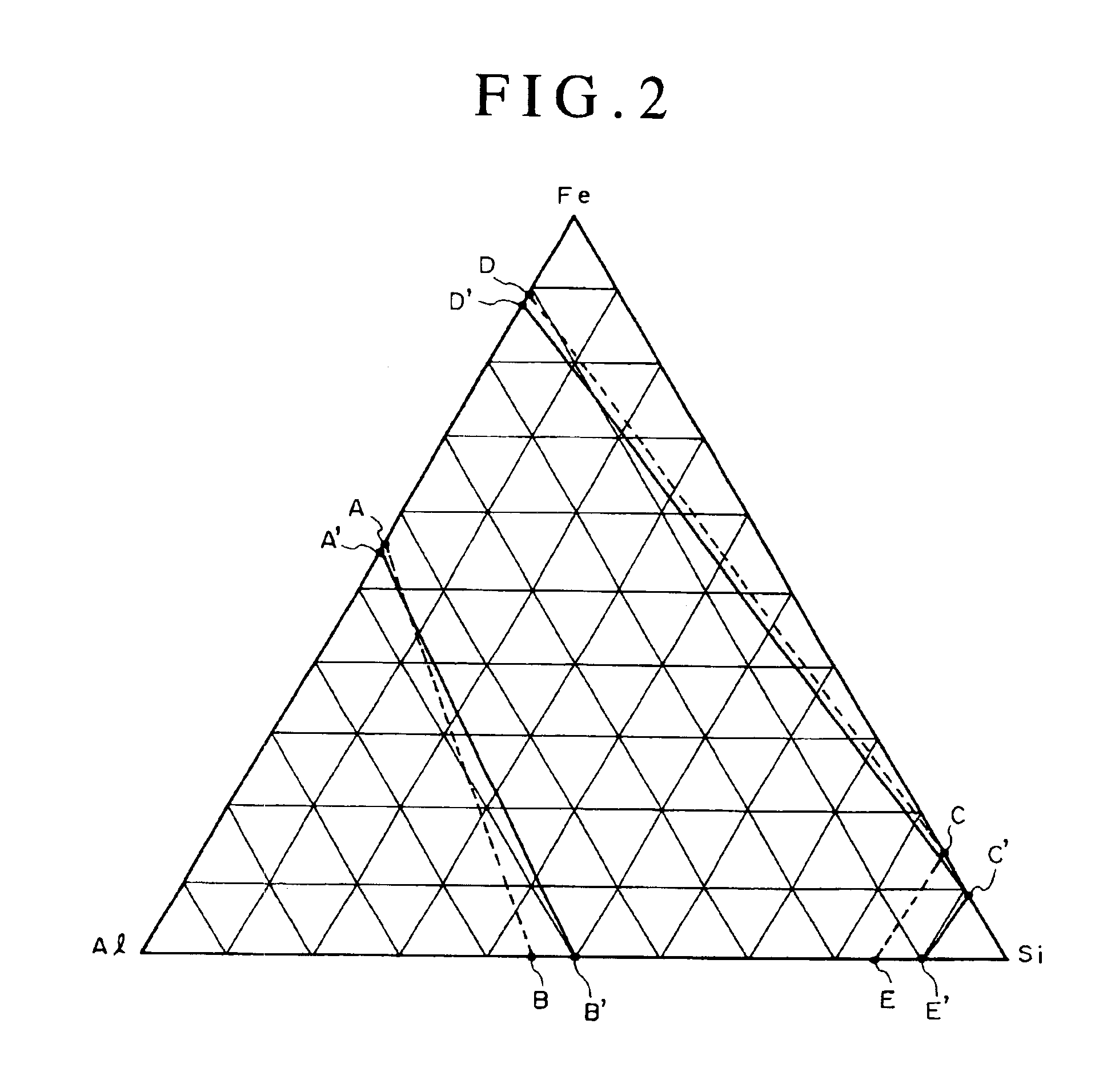
[0136]A disk-like polycarbonate substrate having a thickness of 1.1 mm and a diameter of 120 mm and formed with grooves and lands on the surface thereof was first fabricated by an injection molding process so that the track pitch (groove pitch) was equal to 0.32 μm.

[0137]Then, the polycarbonate substrate was set on a sputtering apparatus and a reflective layer consisting of an alloy containing Ag, Pd and Cu and having a thickness of 100 nm, a second dielectric layer containing a mixture of ZnS and SiO2 and having a thickness of 35 nm, a recording layer containing as a primary component an alloy containing Fe and Al and having a thickness of 10 nm and a first dielectric film containing the mixture of ZnS and SiO2 and having a thickness of 20 nm were sequentially formed on the surface of the polycarbonate substrate on which the grooves and lands were formed, using the sputtering process.

[0138]The mole...


PUM

PropertyMeasurementUnit
thicknessaaaaaaaaaa
outer diameteraaaaaaaaaa
wavelengthaaaaaaaaaa

Abstract

An optical recording medium includes a recording layer containing as a primary component an alloy containing at least two elements selected from the group consisting of Fe, Al and Si and the alloy contained in the recording layer as a primary component has a composition [x1, y1, z1] in terms of the ternary composition diagram that falls within a region of a pentagon defined by straight lines connecting points [57, 43, 0], [0, 55, 45], [15, 0, 85], [89, 11, 0] and [0, 16, 84] in the ternary composition diagram.According to the thus configured optical recording medium, only minimal load is placed on the global environment.

Description

BACKGROUND OF THE INVENTION[0001]The present invention relates to an optical recording medium, a method for manufacturing an optical recording medium and a target used for a sputtering process and, particularly, to an optical recording medium including a recording layer formed of materials that place minimal load on the global environment, a method for manufacturing such an optical recording medium, and a target used for a sputtering process that enables a recording layer of an optical recording medium to be formed of materials that place minimal load on the global environment.DESCRIPTION OF THE PRIOR ART[0002]Optical recording media such as the CD, DVD and the like have been widely used as recording media for recording digital data. These optical recording media can be roughly classified into optical recording media such as the CD-ROM and the DVD-ROM that do not enable writing and rewriting of data (ROM type optical recording media), optical recording media such as the CD-R and DVD...

Claims


Application Information

Patent Timeline
Patent Type & Authority Patents(United States)
IPC IPC(8): C23C14/34G11B7/26B41M5/26G11B7/243G11B7/2433G11B7/2548G11B7/257
CPCC23C14/3414G11B7/243G11B7/266G11B7/258Y10T428/21G11B2007/24306G11B2007/24312G11B7/259
Inventor HOSODA, YASUOMITSUMORI, AYUMISATO, MEGUMIYAMAGUCHI, MASATAKAIIDA, TETSUYAINOUE, HIROYASUMISHIMA, KOJIAOSHIMA, MASAKI
Owner TDK CORPARATION
Why Eureka
Try Eureka