Cross reference to related application

Active Publication Date: 2005-08-16
FUJITSU SEMICON LTD
View PDF7 Cites 7 Cited by
  • Summary
  • Abstract
  • Description
  • Claims
  • Application Information

AI Technical Summary

Benefits of technology

[0025]As described above, according to the present invention, a second insulation film is formed on a first insulation film formed on a substrate and having a copper interconnection layer buried in, a contact hole is formed in the second insulation film down to the copper interconnection layer, the substrate with the contact hole fo

Problems solved by technology

In logic devices having such multi level interconnection, interconnection delay is becoming one dominant factor for signal delay of the devices.
Accordingly, as the size of the contact hole is more reduced, the spin drying finds it difficult to sufficiently dry the interior of the contact hole.
In this case, when the drying after the cleaning is insufficient, the alkaline chemical liquid remaining in the contact hole even after the drying processing acts on the chemical amplification-type resist as an acid deactivating material.
Resultantly, as shown in FIG. 14C, the chemical amplification-type resist film 116 formed on the insulation film 108 has a patterning defect due to the tailing phenomena, and an undesirable condition that the patterning of high precision is difficult will take place.
Furthermore, the deteriorated Cu surface layer 118 is a cause for defective contact.
However, when an insulation

Method used


Image

  • Cross reference to related application
  • Cross reference to related application
  • Cross reference to related application

Examples


Example

[0044][The Principle of the Present Invention]

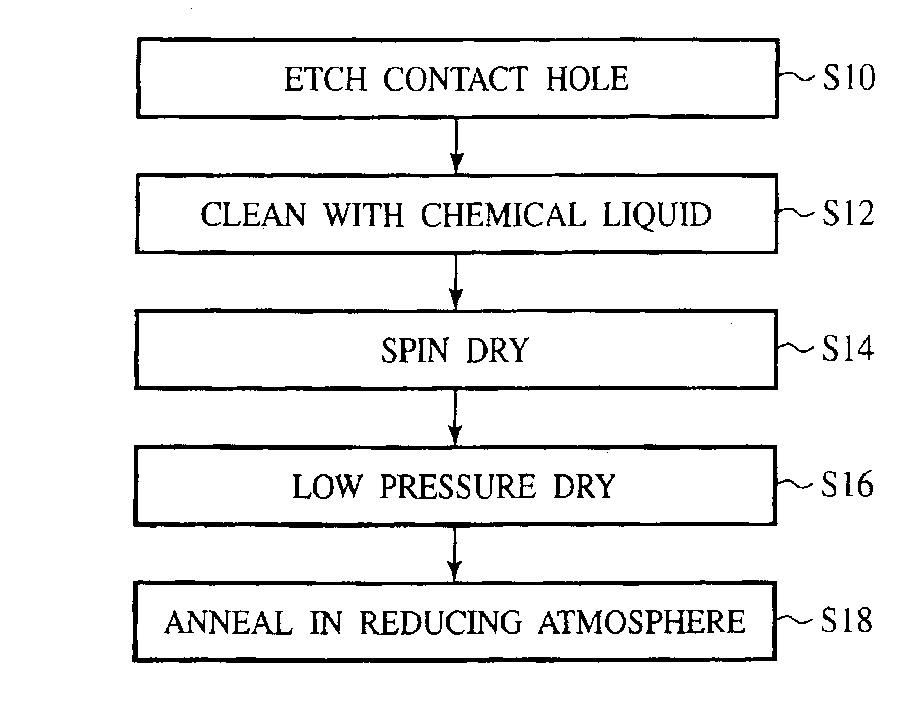
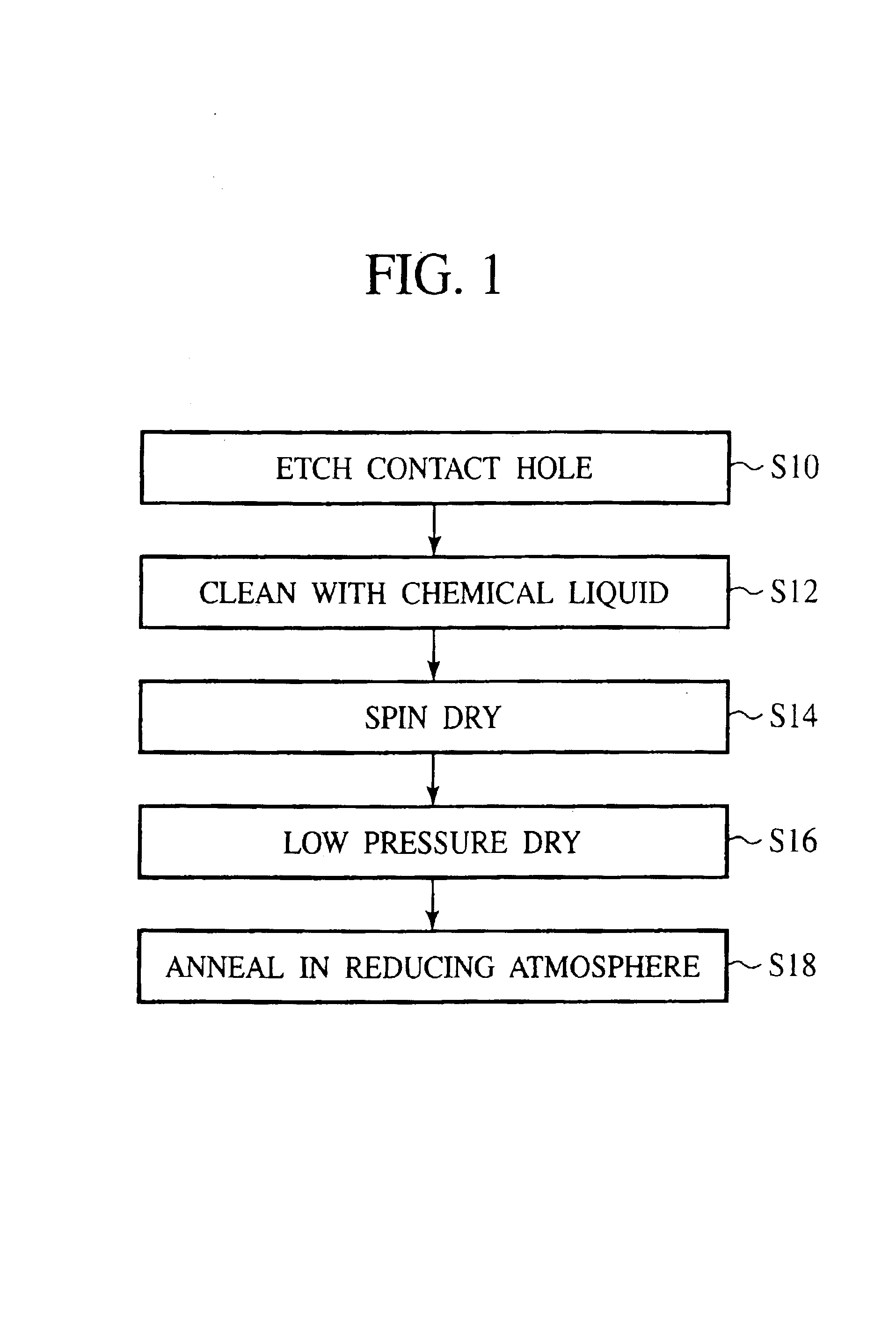
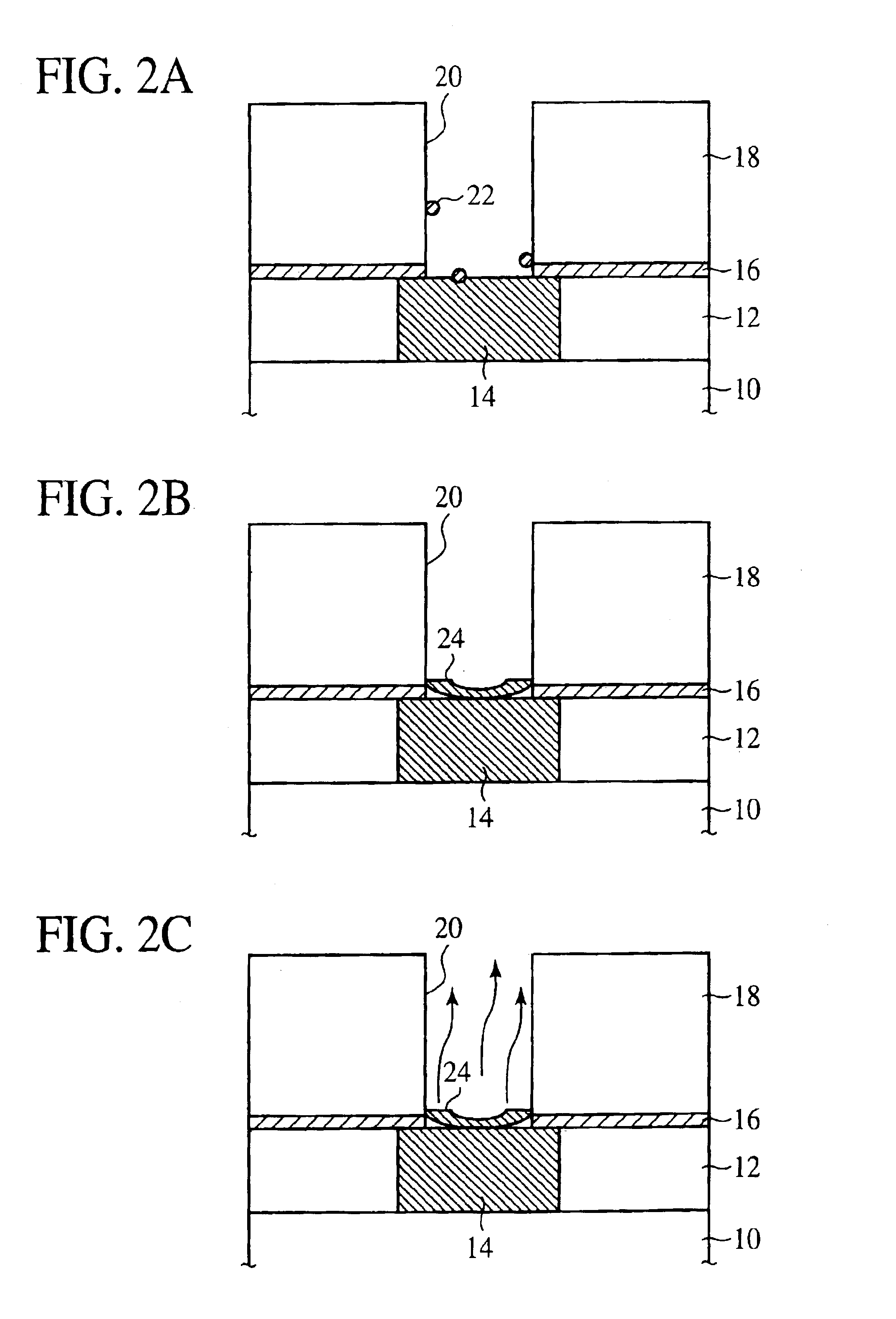
[0045]First, the principle of the method for fabricating a semiconductor device according to the present invention will be explained with reference to FIGS. 1, 2A-2C and 3. FIG. 1 is the flow chart of the method for fabricating a semiconductor device. FIGS. 2A-2C are sectional views of the semiconductor device in the steps of the method for fabricating the semiconductor device according to the present invention, which explain the principle. FIG. 3 is a sectional view of the semiconductor device, which shows a void formed by the migration of Cu in annealing.

[0046]In the method for fabricating a semiconductor device according to the present invention, in the step of forming a Cu interconnection layer, as shown in FIG. 1, the step S10 of forming a contact hole in an insulation film down to the Cu interconnection layer by etching, the step S12 of cleaning with a chemical liquid, the step S14 of drying the contact hole by spin drying, the ste...


PUM


Abstract

The method comprises the step of forming a diffusion preventing film 16 and an insulation film 18 on an insulation film 12 formed on a substrate 10 and having a Cu interconnection layer 14 buried in; the step of forming a contact hole 20 in the insulation film 18 down to the Cu interconnection layer 14; the step of cleaning the substrate 10 with the contact hole 20 formed with a chemical liquid; the step of drying the substrate 10 cleaned with the chemical liquid; and the step of annealing the dried substrate in a reducing atmosphere.

Description

CROSS-REFERENCE TO RERATED APPLICATION[0001]This application is based upon and claims priority of Japanese Patent Application No. 2002-252890, filed on Aug. 30, 2002, the contents being incorporated herein by reference.BACKGROUND OF THE INVENTION[0002]The present invention relates to a method for fabricating a semiconductor device using copper as an interconnection material.[0003]Higher integration of semiconductor cells and downsizing of chips have accelerated the micronization of the interconnection, and the multi level interconnection. In logic devices having such multi level interconnection, interconnection delay is becoming one dominant factor for signal delay of the devices.[0004]The interconnection delay, which is becoming one factor for the signal delay of the devices has a proportional relationship with a product of an interconnection resistance with an interconnection capacitance. Accordingly, to decrease the interconnection delay it is important to decrease the interconne...

Claims


Application Information

Patent Timeline
IPC IPC(8): H01L21/70H01L21/768H01L21/306H01L21/312
CPCH01L21/76802H01L21/76811H01L21/76813H01L21/76814
Inventor IKEDA, MASANOBU
Owner FUJITSU SEMICON LTD
Why Eureka
Try Eureka