Semiconductor circuit and method of fabricating the same

a semiconductor and circuit technology, applied in the direction of semiconductor devices, electrical devices, transistors, etc., can solve the problems of reducing the production efficiency of semiconductor films, so as to reduce the variation between semiconductor circuits (analog circuits) and the plurality of semiconductor devices.

Inactive Publication Date: 2005-08-16
SEMICON ENERGY LAB CO LTD
View PDF83 Cites 49 Cited by
  • Summary
  • Abstract
  • Description
  • Claims
  • Application Information

AI Technical Summary

Benefits of technology

[0013]Another object of the present invention is to form a plurality of semiconductor devices which require high conformity from crystalline semiconductor films with uniform crystallinity, further to provide a semiconductor circuit in which variation between semiconductor devices is small and a semiconductor integrated circuit with high performance.
[0024]As the laser light or the strong light which is concentrated in a line shape and expanded in a long direction is irradiated to the semiconductor film, a position of laser light irradiation and a substrate on which the crystalline semiconductor films are formed move relatively, and the semiconductor films are melted by scanning a part or whole thereof by the laser light, and through that situation, crystallization or recrystallization is carried out. The scanning direction of the laser light is along a long direction of the depression formed in the insulating film and extending as a liner stripe pattern or a channel length direction of the transistor. By this, crystals are grown along the scanning direction of the laser light, and it is possible to prevent crystal grain boundaries from crossing the channel length direction.
[0027]By setting depth of the depression as the same level or more as thickness of the semiconductor film, the semiconductor film which is melted by irradiation of the laser light or the strong light is coagulated and solidified in the depression due to surface tension. As a result, the thickness of the semiconductor film located on the projection of the insulating film gets thinner so that it is possible to localize stress-strains on it. Also, a side surface of the depression has an effect for defining crystal orientation to some degree.
[0033]According to the invention, on the insulating surface, in particular, on the insulating surface in case that an inexpensive glass substrate is used as a support substrate, the channel forming regions are formed from the stripe-shaped crystalline semiconductor films on the same line so that variation between a plurality of semiconductor devices can be reduced, and further, variation between semiconductor circuits (analog circuits) can be reduced, and it is possible to provide a high-performance semiconductor integrated circuit. In addition, two or more semiconductor circuits gather to form the semiconductor integrated circuit, and the semiconductor circuit has semiconductor devices comprising thin film transistors in which at least conformity is required.

Problems solved by technology

However, when crystallization is made by irradiating the laser beams onto the amorphous semiconductor film, the crystal includes poly-crystals, producing defects such as a grain boundary which is formed at random.
Therefore, it becomes difficult to obtain uniform crystallinity and crystal orientations.
Crystal defects are involved in a grain boundary, resulting in a carrier trap.
Also, it is impossible to form a semiconductor film with neither distortion nor crystal defects due to a volume shrinkage of the semiconductor films, a thermal stress applied between the semiconductor film and a base film, or lattice mismatching, accompanied with crystallization.
Consequently, the distortion and crystal defects produce causative factors of not only variation of electrical characteristics of the semiconductor device, but also inferior electrical characteristics of the semiconductor device.
Especially when crystalline semiconductor films are formed by using laser beams on a non-alkali glass substrate used abundantly and industrially, the focuses of the laser beams varies in response to the influence of the surge of the non-alkali glass substrate itself, involving a problem of causing crystalline variation as a result.
The semiconductor integrated circuit and the like have semiconductor films formed on cheap glass substrates to constitute transistors, therefore, it is almost impossible to arrange transistors so as to aovid grain boundaries formed at random.
That is, the grain boundaris or crystal defects involved unexpectedly could not be eliminated by controlling strictly the crystallinity of the channel forming regions of transistors.
This produced a causative factor of variation of electrical characteristics of the semiconductor device, thus, it is difficult to form a circuit which requires high conformity (for example, a current mirror circuit).

Method used


Image

  • Semiconductor circuit and method of fabricating the same
  • Semiconductor circuit and method of fabricating the same
  • Semiconductor circuit and method of fabricating the same

Examples


embodiment 1

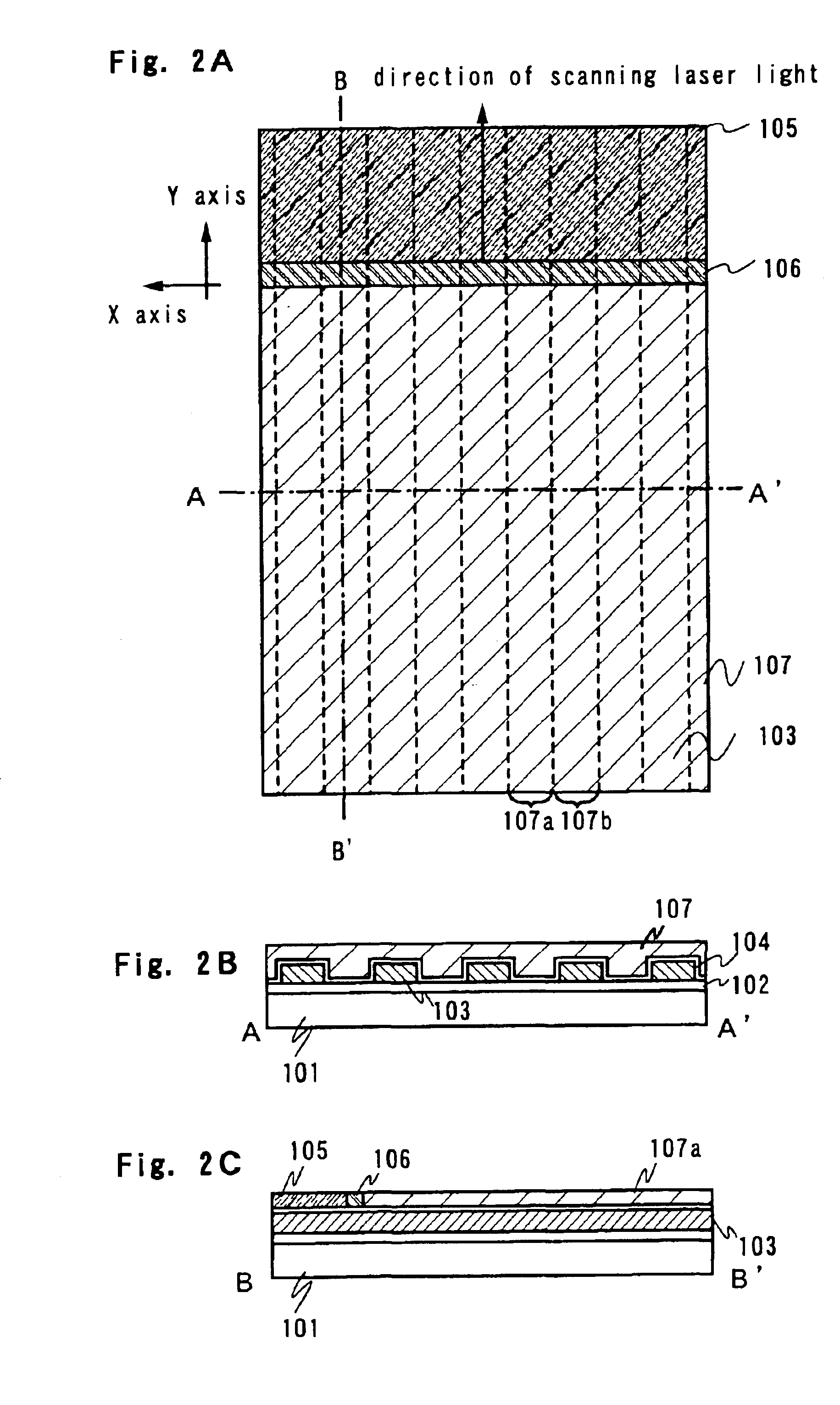
[0055]In this embodiment, a manner for fabricating a thin film transistor by carrying out the invention will be described. Also, in FIGS. 3 to 6, it is described that there are two thin film transistors on the same stripe but, the number of the thin film transistors to be formed may be determined appropriately by a person who carries out it, and any of the figures used does not give any limitations to the invention.

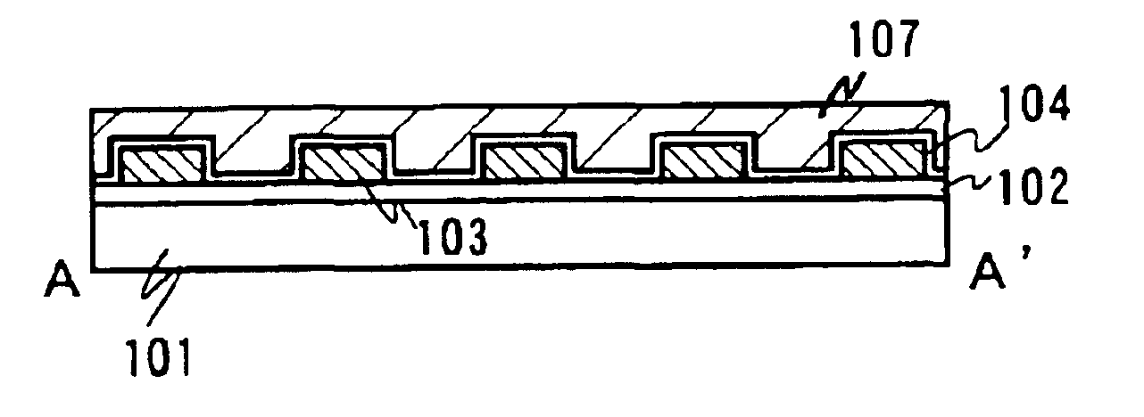
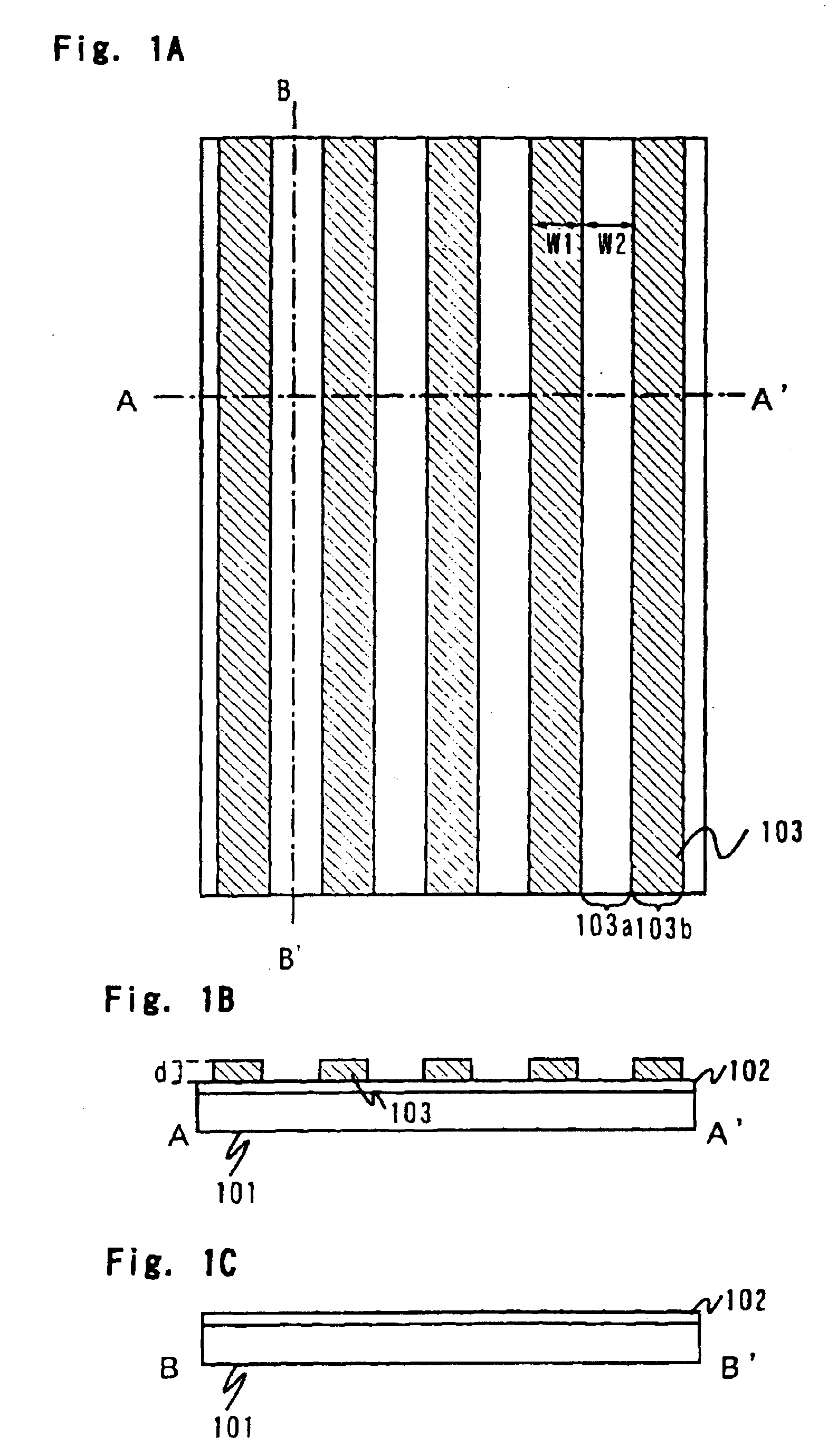
[0056]Firstly, FIGS. 1A to 1C will be described. FIG. 1A is a top view, and FIG. 1B is a sectional view corresponding to A-A′. It shows a situation that, on a substrate 101, a first insulating film 102 and a second insulation firm 103 which is formed in a linear stripe pattern are formed. In addition, in the embodiment, a depression designates a portion shown by 103a, and a projection designates a portion shown by 103b.

[0057]As the substrate 101, a commercially available non-alkali glass substrate, a quartz substrate, a sapphire substrate, a substrate which is formed by ...

embodiment 2

[0115]As a formation method of the crystalline semiconductor film of this invention, as shown in the embodiment 1, melting and recrystallization may be satisfactory by irradiating laser beams further after crystallization by solid phase growth, other than the method which irradiates laser beams onto an amorphous semiconductor film to crystallize.

[0116]For example, after an amorphous semiconductor film 105 is formed in FIG. 2, nickel is doped as metallic elements with catalyst effect to promote crystallization in such a way that the crystallization temperature of the amorphous semiconductor film (for example, amorphous silicon film) is lowered, and the orientation thereof is raised.

[0117]This technique is described in detail in JP-A-11-354442 by this applicant. A crystalline semiconductor film obtained by combining a technique of doping nickel and the technique in Embodiment 1 also has a characteristic of uniform crystallinity. If such crystalline semiconductor films are used for the...

embodiment 3

[0123]Next, by use of FIG. 8, an example will be described, in which length of the stripe pattern is such level of length that the channel forming region of the transistor can be formed.

[0124]FIG. 8 is a top view, and FIG. 8B is a sectional view corresponding to A-A′, and FIG. 8C is a sectional view corresponding to C-C′. They shows such a situation that a first insulating film 802 and a second insulating film 803 formed in linear stripe patterns are formed on a substrate 801. In addition, a portion shown by 803a indicates a depression, and a portion shown by 803b indicates a projection.

[0125]A feature of this embodiment is that the length of the linear stripe pattern is set to be such a level that a channel forming region are of a transistor can be formed. That is, looking at the sectional view of A-A′, the second insulating film 803 is not disposed, and looking at the sectional view of C-C′, the second insulating film 803 is disposed in a stripe shape. Also, the first insulating f...


PUM


Abstract

According to the invention, a plurality of semiconductor devices which are required to have conformance are formed from crystalline semiconductor films having uniform crystallinity on the same line, and a semiconductor circuit in which variation between semiconductor devices is small can be provided, and a semiconductor integrated circuit having high conformance can be provided. The invention is characterized in that, in a part or whole of thin film transistors which configure an analog circuit such as a current mirror circuit, a differential amplifier circuit, or an operational amplifier, in which high conformance is required for semiconductor devices included therein, channel forming regions have crystalline semiconductor films on the same line. High conformance can be expected for an analog circuit which has the crystalline semiconductor films on the same line formed using the invention as the channel forming regions of the thin film transistors. That is, the invention is characterized in that, among the thin film transistors which configures the analog circuit, the channel forming regions of the thin film transistors having at least the same polarity are formed on the same line.

Description

BACKGROUND OF THE INVENTION[0001]1. Field of the Invention[0002]The present invention relates to a semiconductor device which is formed by using a semiconductor film having a crystal structure (also referred to as a crystalline semiconductor film) and a method for manufacturing the same, as well as a semiconductor integrated circuit equipped with a circuit integrating the semiconductor devices and a method for manufacturing the same. Further, the present invention relates to a semiconductor device having a plurality of the semiconductor integrated circuits. And, the present invention especially relates to a thin film transistor which forms a channel forming region by a crystalline semiconductor film formed on an insulating surface as a semiconductor device.[0003]2. Description of the Related Art[0004]A technique for forming a semiconductor device such as a thin film transistor and the like using a crystalline semiconductor film formed on an insulation substrate such as glass, has be...

Claims


Application Information

Patent Timeline
Patent Type & Authority Patents(United States)
IPC IPC(8): H01L21/02H01L21/70H01L29/786H01L21/336H01L29/66H01L27/12H01L21/84H01L21/77
CPCH01L27/12H01L29/66757H01L29/78675H01L29/78696H01L27/1281H01L21/2026H01L21/02686H01L21/0242H01L21/02683H01L21/02691H01L21/02425H01L21/02488H01L21/02422H01L21/02672H01L21/02532H01L21/02678H01L21/02502
Inventor KATO, KIYOSHIATSUMI, TOMOAKIISOBE, ATSUO
Owner SEMICON ENERGY LAB CO LTD
Why Eureka
Try Eureka