Supercharge Your Innovation With Domain-Expert AI Agents!

Nonvolatile memory and method of programming the same memory

Inactive Publication Date: 2005-08-16
RENESAS ELECTRONICS CORP
View PDF8 Cites 13 Cited by
  • Summary
  • Abstract
  • Description
  • Claims
  • Application Information

AI Technical Summary

Benefits of technology

[0009]It is therefore an object of the present invention to provide a non-volatile memory such as a flash memory that can reduce the total write operation time.
[0025]Moreover, the directions of a write current of the selected memory cell and a read current to verify the write operation are set identical to the direction of current flowing into the selected memory cells during the write operation. Thereby, data read operation can be performed accurately by avoiding that the threshold voltages of memory cells are different depending on the current flowing direction.

Problems solved by technology

Accordingly, there arises a problem that a load capacitance of bit line becomes larger, the time required until the bit line reaches the predetermined potential becomes larger, and thereby the time required for write operation also becomes longer and power consumption also becomes high.
Moreover, when the write system by the FN tunnel is employed, there exists a problem that the scale-down of memory element becomes difficult and integration degree cannot be improved because an element isolation region must be provided among the cells for insulation between memory cells and the dielectric strength of elements forming a memory cell must be further raised in comparison with the hot-electron system.

Method used


Image

  • Nonvolatile memory and method of programming the same memory
  • Nonvolatile memory and method of programming the same memory
  • Nonvolatile memory and method of programming the same memory

Examples


Embodiment Construction

[0043]A preferred embodiment of the present invention will be explained with reference to the accompanying drawings.

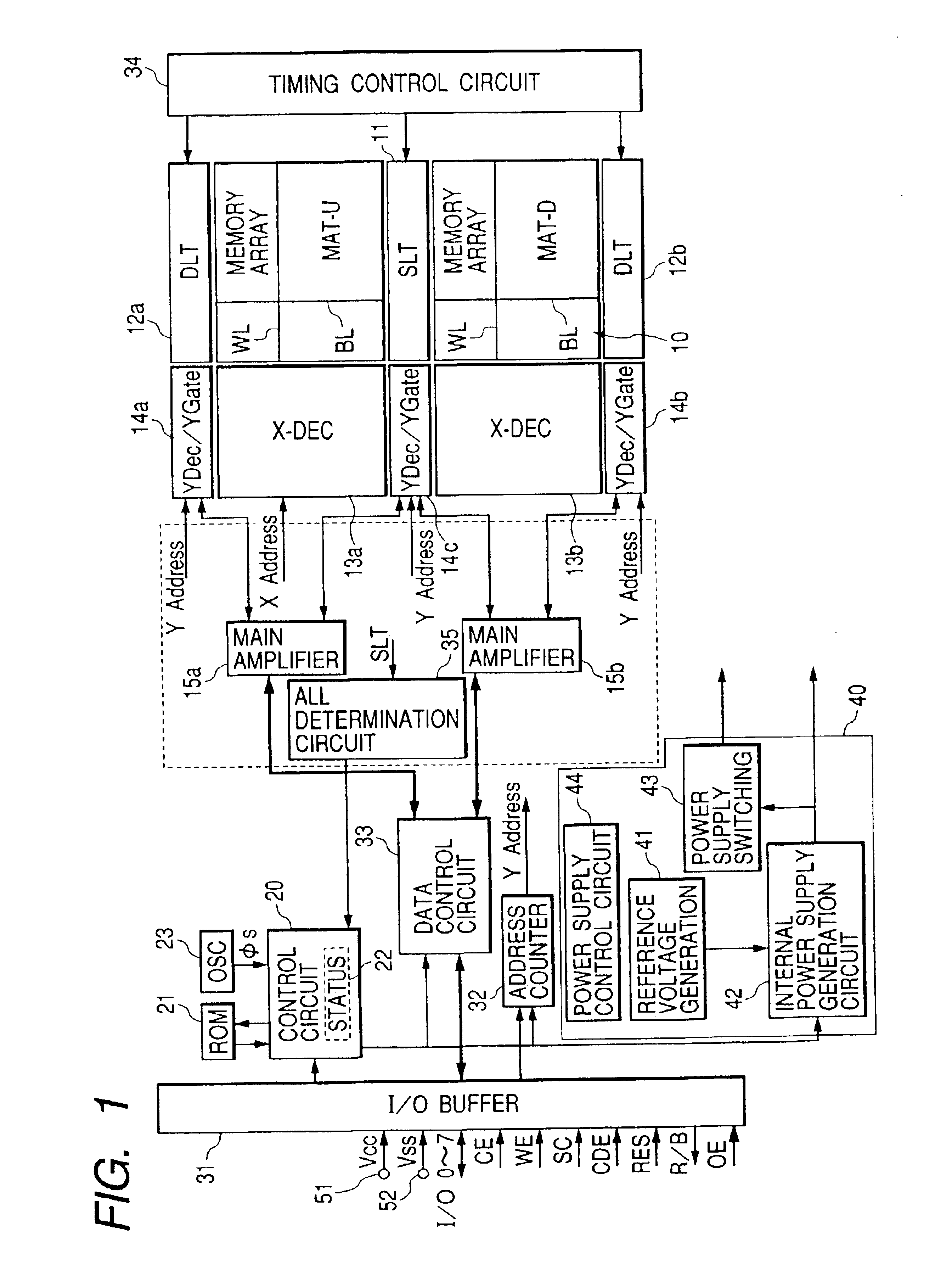
[0044]FIG. 1 is a block diagram of an example of a flash memory as a non-volatile storage device to which the present invention is adapted. Although not particularly restricted, the flash memory of FIG. 1 is structured as a multi-level memory for storing the data of 2-bits in each memory cell and is formed on one semiconductor chip such as a single crystal silicon.

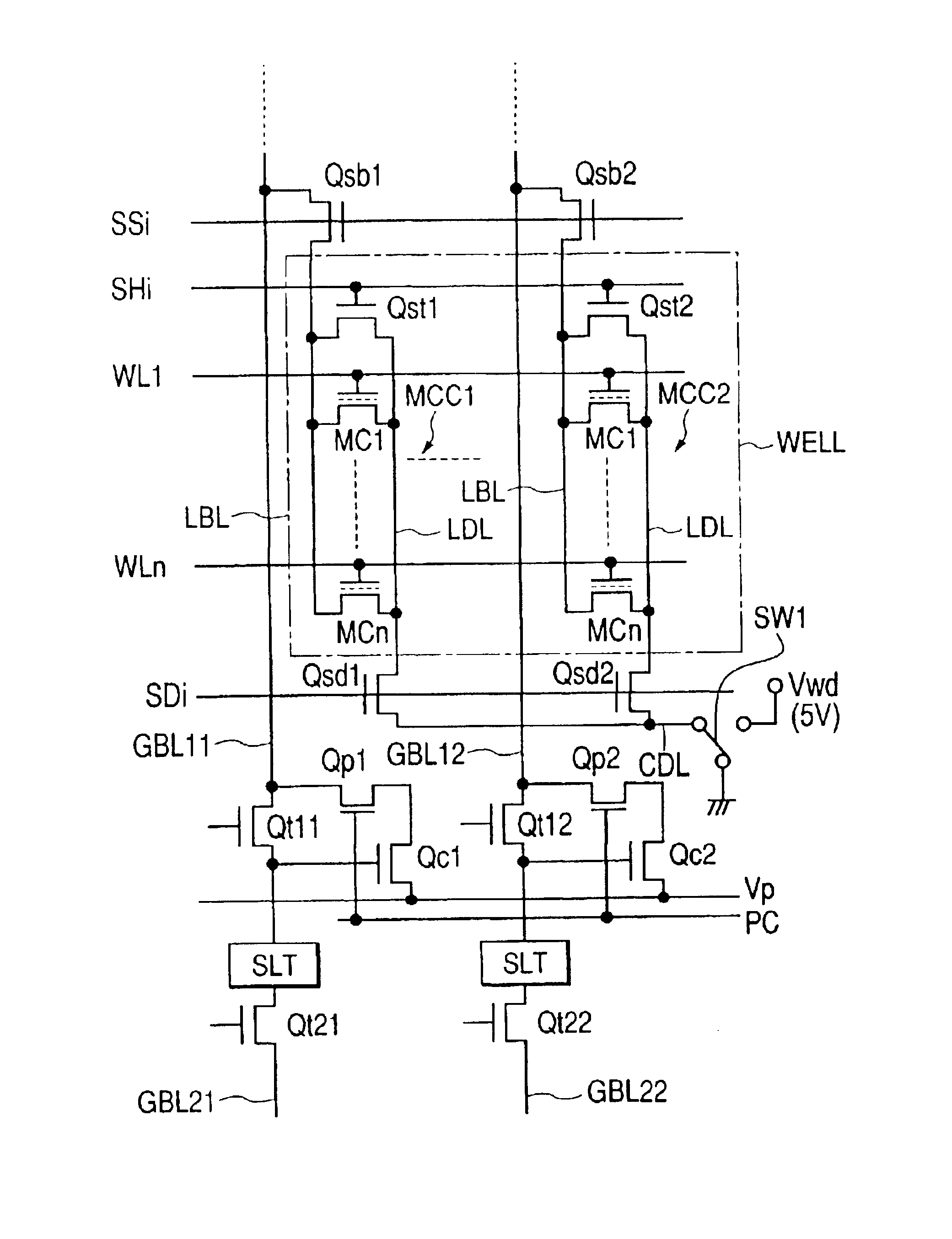
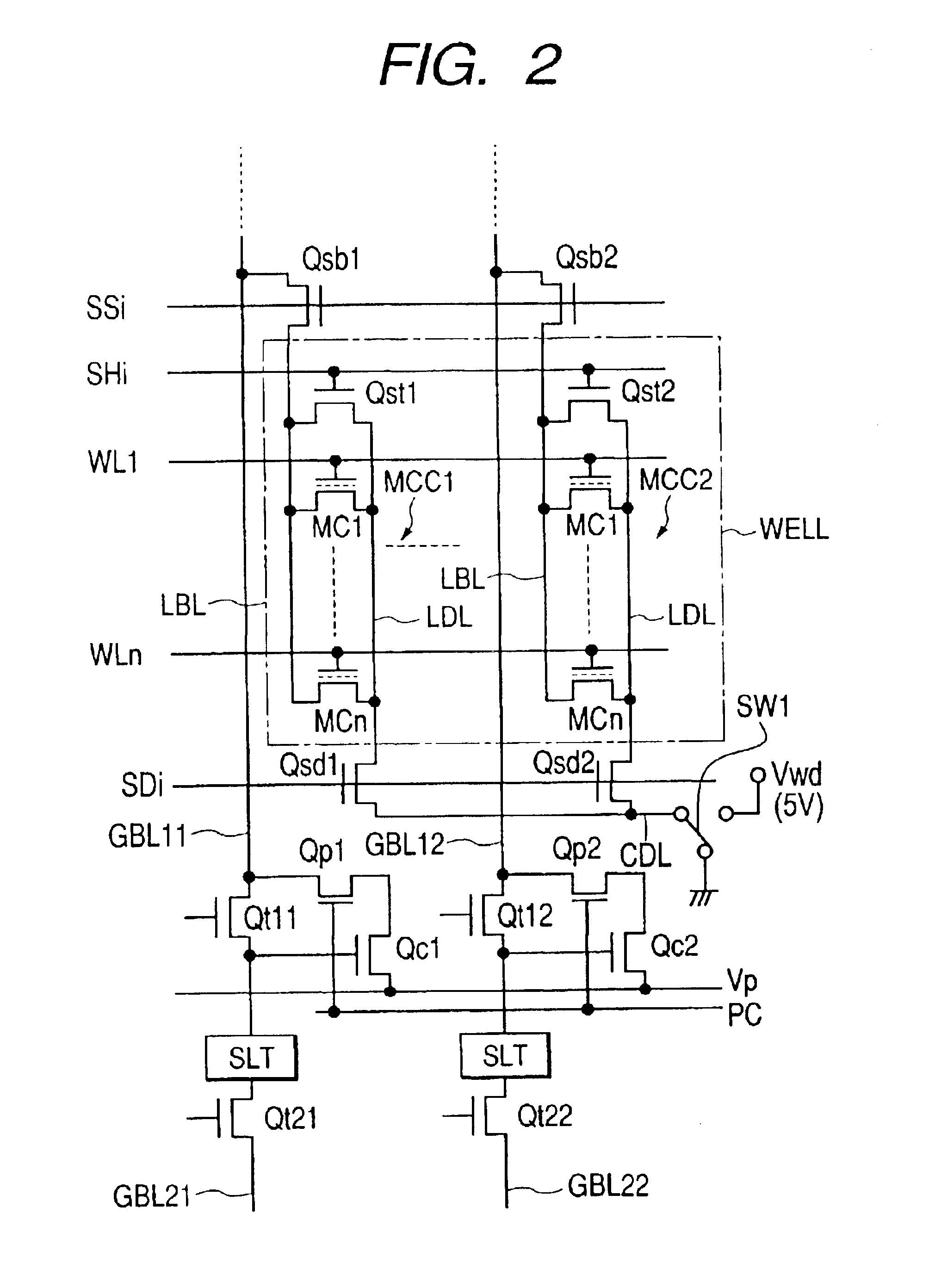
[0045]Although not particularly restricted, in the flash memory of FIG. 1, a memory array 10 is structured with two memory mats MAT-U, MAT-D and a sense latch circuit 11 is placed between the mats for amplifying and latching a read signal connected to the bit line BL in each mat and precharging the bit line. A part of this sense latch circuit 11 for amplifying operation and latch operation is called the sense latch and is expressed as SLT. Moreover, data latch circuits 12a, 12b for temporarily holding the rea...


PUM


Abstract

There is provided a method of programming a non-volatile memory which can solve the problem of the data write system of the existing flash memory that a load capacitance of bit lines becomes large, the time required by the bit lines to reach the predetermined potential becomes longer, thereby the time required for data write operation becomes longer and power consumption also becomes large because the more the memory capacitance of memory array increases, the longer the length of bit lines becomes and the more the number of bit lines increases. In the non-volatile memory of the invention comprising the AND type memory array in which a plurality of memory cells are connected in parallel between the local bit lines and local drain lines, the local drain lines are precharged by supplying thereto a comparatively higher voltage from the common drain line side (opposite side of the main bit lines), the main bit lines are selectively precharged by applying thereto the voltage of 0V or a comparatively small voltage depending on the write data and thereafter a drain current is applied only to the selected memory cells to which data is written by applying the write voltage to the word lines in order to implant the hot electrons to the floating gate.

Description

CROSS-REFERENCE TO RELATED APPLICATION[0001]This application is a continuation of application Ser. No. 10 / 012,549 filed Dec. 12, 2001 now U.S. Pat. No. 6,567,315.BACKGROUND OF THE INVENTION[0002]The present invention relates to a technique that can be effectively adapted to a write control system in an electrically erasable and programmable non-volatile memory and more specifically to a technique that can be effectively adapted to a flash memory being capable of simultaneously erasing data, for example, in a predetermined unit.[0003]A flash memory uses, as a memory cell, a non-volatile memory element consisting of a MOSFET of the double-gate structure including a control gate and a floating gate. The write system in the flash memory has been sorted to a system utilizing the FN tunnel phenomenon and a hot-electron system. In the system utilizing the FN tunnel phenomenon, a voltage is applied across the control gate and substrate (or well region) or across the control gate and source ...

Claims


Application Information

Patent Timeline
IPC IPC(8): G11C16/12G11C16/06G11C16/02G11C11/56G11C16/04G11C16/10
CPCG11C11/5628G11C16/10G11C16/12G11C16/3459G11C16/06
Inventor TAKASE, YOSHINORIKUBONO, SHOJIKANAMITSU, MICHITARONOZOE, ATSUSHIYOSHIDA, KEIICHIKURATA, HIDEAKI
Owner RENESAS ELECTRONICS CORP
Features
  • R&D
  • Intellectual Property
  • Life Sciences
  • Materials
  • Tech Scout
  • Unparalleled Data Quality
  • Higher Quality Content
  • 60% Fewer Hallucinations
Learn More