Conductor-within-a-via microwave launch

a conductor and a technology of a via, applied in the field of communication systems, can solve the problems of rf pass-through loss, leakage to one or more internal layers of printed circuit conductor traces, and degrade the voltage standing wave ratio (vswr)

Inactive Publication Date: 2005-08-30
NORTH SOUTH HLDG
View PDF6 Cites 42 Cited by
  • Summary
  • Abstract
  • Description
  • Claims
  • Application Information

AI Technical Summary

Benefits of technology

[0004]In accordance with the present invention, problems of conventional RF feed-throughs, such as those described above, are effectively obviated by a concentric ‘conductor within a via’ RF interconnect architecture, having an inner co

Problems solved by technology

A problem with this approach is the relatively poor shielding offered by the ‘punctuated’ arrangement of spaced apart ground vias, which typicaly results in leakage to one or more internal layers of printed circuit conductor traces.
In addition, the feed-through suffers from transition

Method used


Image

  • Conductor-within-a-via microwave launch
  • Conductor-within-a-via microwave launch
  • Conductor-within-a-via microwave launch

Examples


Embodiment Construction

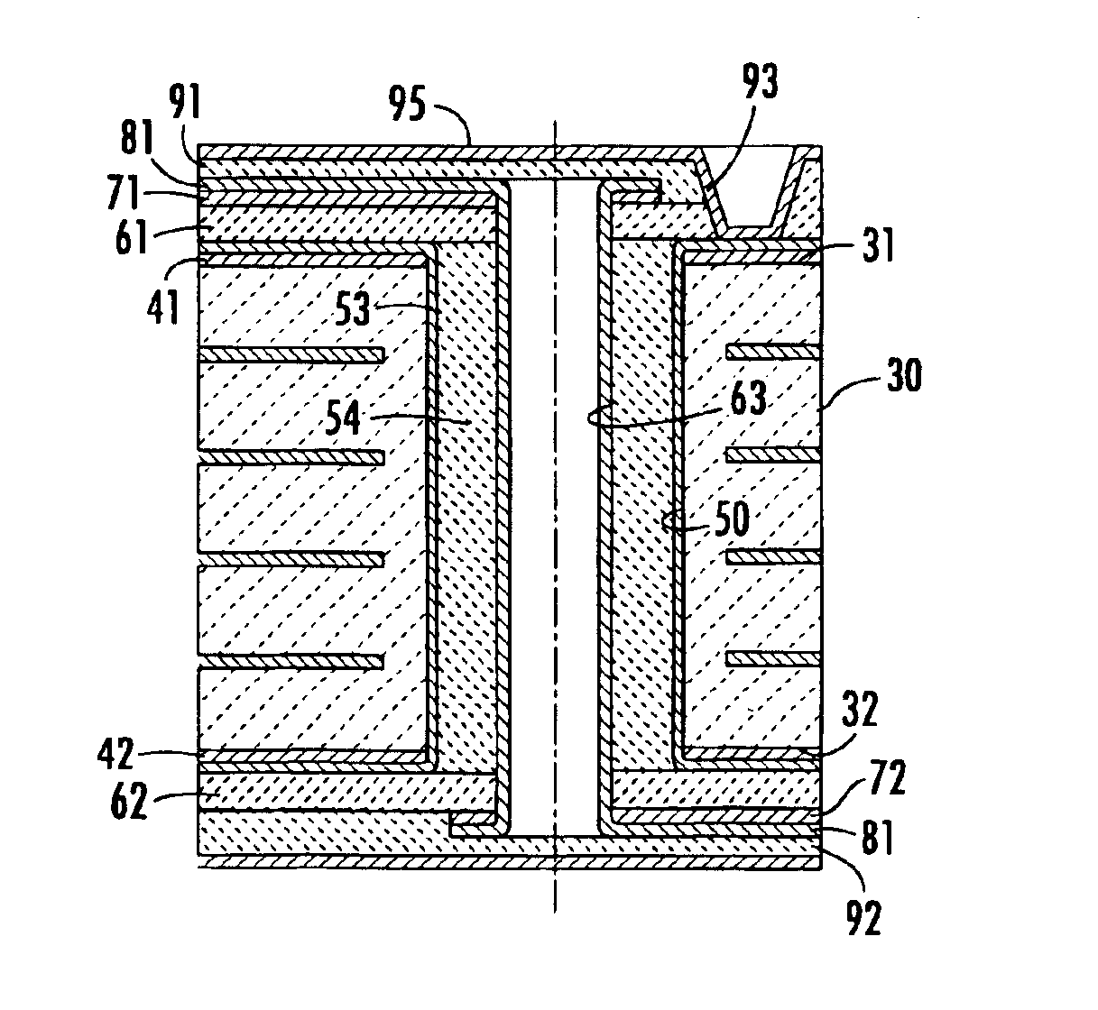
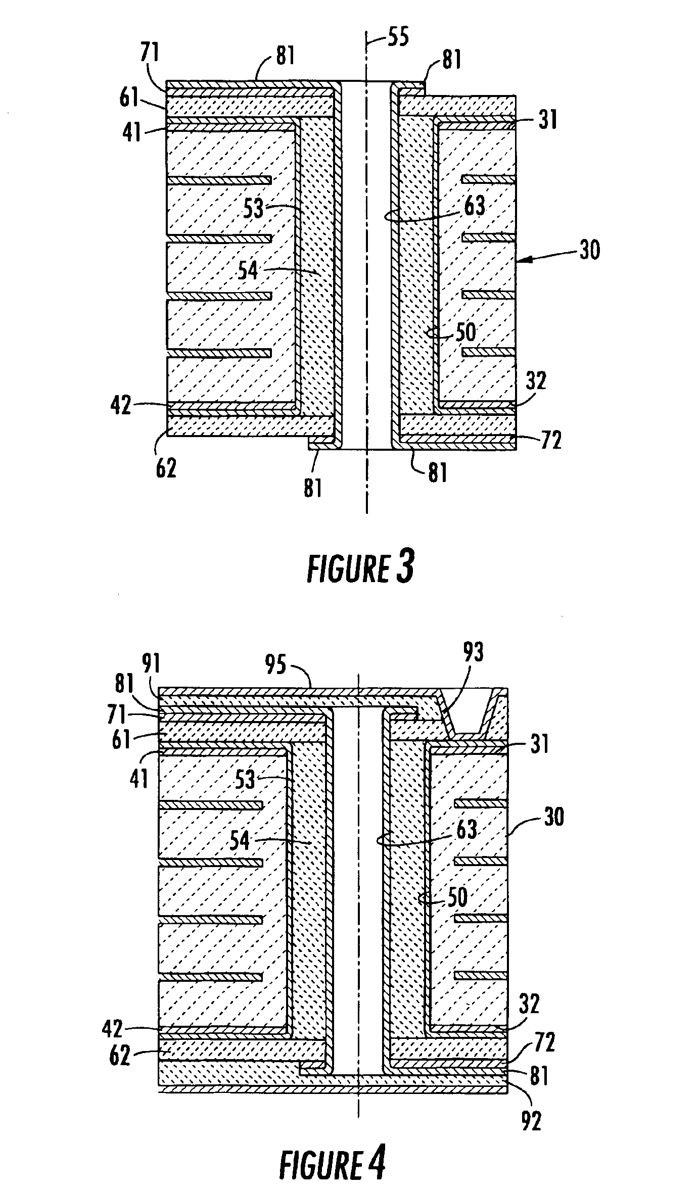
[0015]A first microstrip-coupling embodiment of the improved conductor within a via, shielded microwave interconnect structure in accordance with the present invention is diagrammatically illustrated in FIG. 3 as comprising a substrate 30 having first and second, generally parallel, opposite planar surfaces 31 and 32, and containing a laminate structure of multiple printed circuit layers therein. A first ground plane layer 41 is formed on the first planar surface 31, while a second ground plane layer 42 is formed on the second surface 32. A first, outer via or aperture 50 (which may be formed as a drilled cylindrical through hole) extends through the substrate 30 along an axis 55, so that it intersects the ground plane layers 41 and 42 on the respective opposite surfaces 31 and 32.

[0016]A conductive material is formed on the first and second ground plane layers 41 and 42, respectively, and also on the (generally cylindrical) sidewall of the aperture 50. In addition to thickening the...


PUM


Abstract

A concentric ‘conductor within a via’ RF interconnect architecture, has an inner via through which at least one RF signal conductor passes. The inner conductive via is coaxially formed within and stably coaxially aligned within an outer conductive via, which serves as a coaxial ground plane that completely surrounds the inner conductive via. The outer conductive via passes through dielectric layers of microstrip or stripline structures on opposite sides of a multi printed circuit laminate.

Description

FIELD OF THE INVENTION[0001]The present invention relates in general to communication systems and components therefor, and is particularly directed to a new and improved ‘conductor-within-a-via’, microwave interconnect structure for use with laminated radio frequency (RF) printed circuit architectures.BACKGROUND OF THE INVENTION[0002]Laminated printed circuit architectures employed for RF (microwave / millimeter wave) applications use a variety of feed-through configurations for transporting RF signals between opposite sides of a substrate laminate. One of these structures, shown diagrammatically in plan in FIG. 1, distributes a plurality of ground vias (four being shown at 11, 12, 13 and 14 in FIG. 1) around an RF feed-through pin 15 which, in turn, is connected to a microstrip launch conductor 16. A problem with this approach is the relatively poor shielding offered by the ‘punctuated’ arrangement of spaced apart ground vias, which typicaly results in leakage to one or more internal...

Claims


Application Information

Patent Timeline
IPC IPC(8): H01P5/16H01P3/08H01P5/18H05K1/02H05K1/11H05K3/40H05K3/46H05K3/42H05K3/44H01P1/04
CPCH01P1/047H01P3/081H01P3/085H01P5/184H05K1/0222H05K1/115H05K1/0237H05K3/4046H05K3/429H05K3/445H05K3/4608H05K2201/09536H05K2201/09809H05K2201/10287
Inventor FISHER, CHARLES ROBERTPEDERSEN, ANDERS P.WHYBREW, WALTER M.
Owner NORTH SOUTH HLDG
Why Eureka
Try Eureka