Nonvolatile memory cell and nonvolatile semiconductor memory device

Active Publication Date: 2005-08-30
SAMSUNG ELECTRONICS CO LTD
View PDF6 Cites 118 Cited by
  • Summary
  • Abstract
  • Description
  • Claims
  • Application Information

AI Technical Summary

Benefits of technology

[0021]Furthermore, according to the characteristic configuration, because each bit line is charged up to a predetermined potential before the reading operation, the reading operation is accelerated and stabilized, by decreasing the influence of the leak current and mainly reading

Problems solved by technology

Therefore, when other resistances are larger than the resistance of the RRAM element 2, the above bit line difference is relatively decreased and a stable reading operation and high-speed operation become difficult.
Anyway, this is a problem common to nonvolatile memories.
However, when the transistor is connected to each RRAM e

Method used


Image

  • Nonvolatile memory cell and nonvolatile semiconductor memory device
  • Nonvolatile memory cell and nonvolatile semiconductor memory device
  • Nonvolatile memory cell and nonvolatile semiconductor memory device

Examples


Example

(First Embodiment)

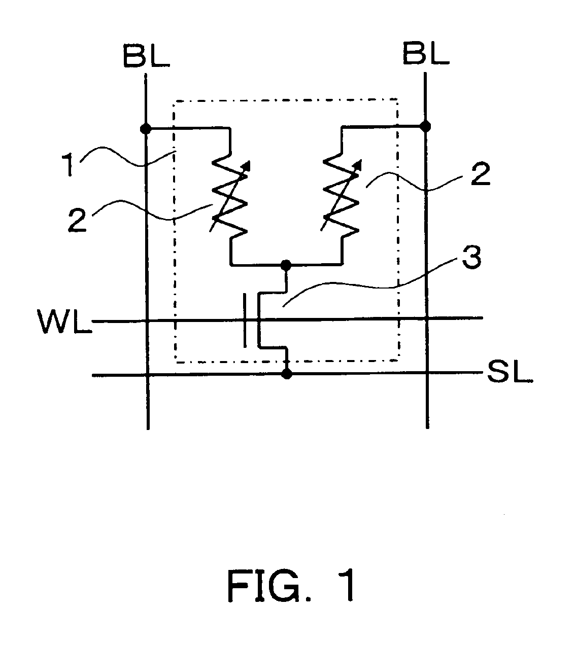
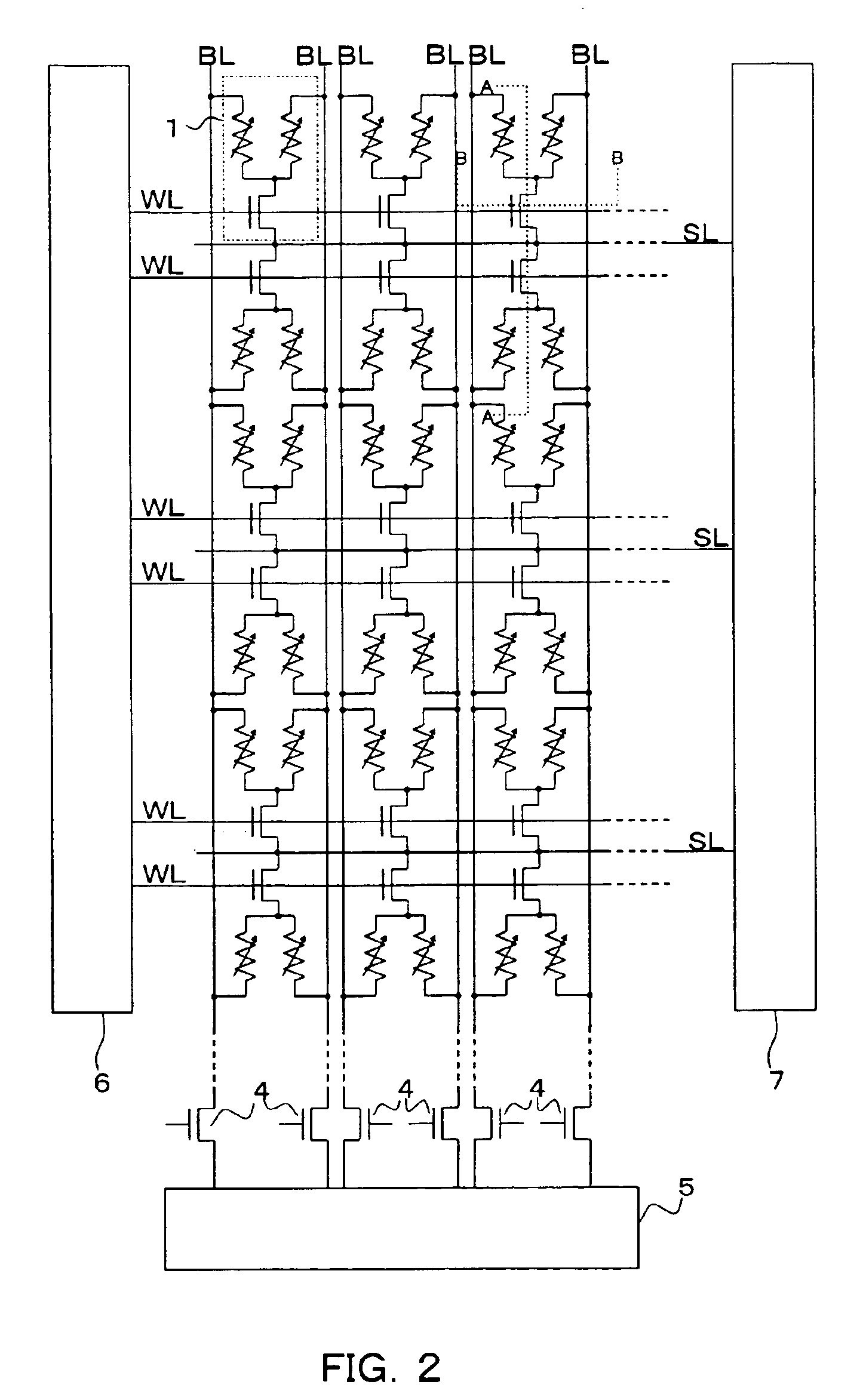
[0048]FIG. 1 shows a configuration of a memory cell 1 of the present invention device. The memory cell 1 has a selection transistor 3 constituted by two variable resistive elements 2 and one N-type MOSFET serving as a selection element for selecting the two variable resistive elements, in which one end of each variable resistive element 2 is connected to the drain electrode of the selection transistor 3. Moreover, other ends of variable resistive elements 2 are connected to different bit lines BL respectively, the gate of the selection transistor 3 are connected to word line WL and the source of the selection transistor 3 is connected to a source line SL. In the case of this embodiment, because one memory cell includes two variable resistive elements 2, there is a memory capacity two times larger than the memory capacity of the conventional memory cell shown in FIG. 17. However, when relating one memory cell to one variable resistive element 2, it can be said that ...

Example

(Second Embodiment)

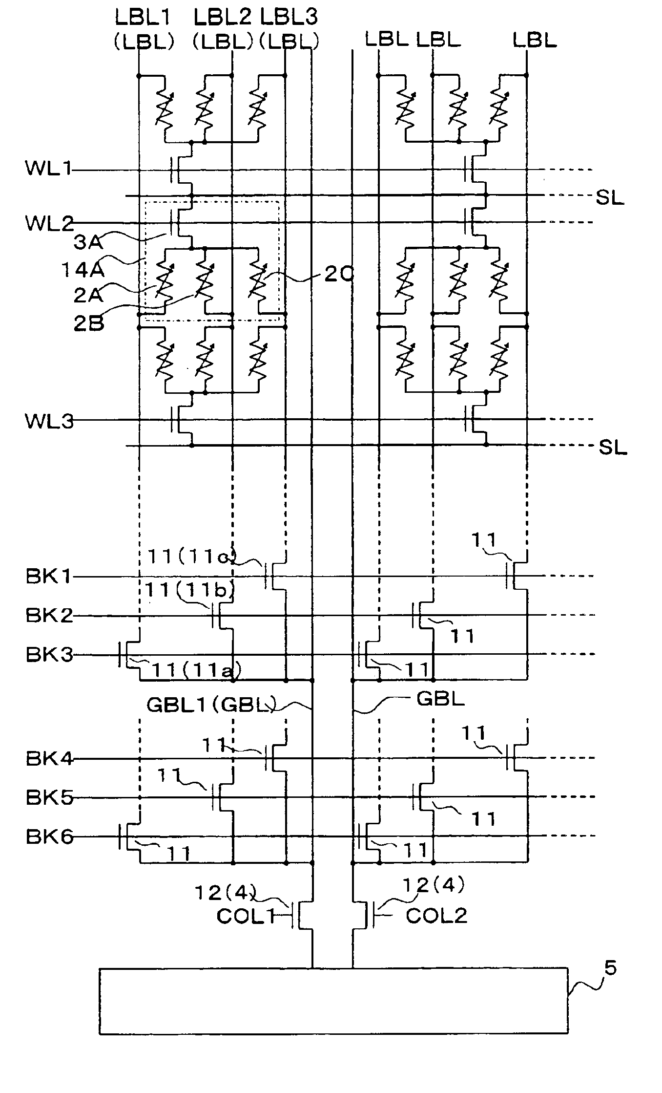
[0052]FIG. 4 shows a memory array configuration using a hierarchical bit line structure on the basis of the memory array configuration shown in FIG. 2 and FIG. 5 shows a reading circuit in the hierarchical bit line structure. To realize stable reading of stored data from a memory cell 1 at a high speed and stability, it is possible to realize a memory array configuration having the hierarchical bit line structure shown in FIG. 4.

[0053]In the case of the hierarchical bit line structure of this embodiment, a bit line directly connected to the memory cell 1 is referred to as a local bit line LBL. A plurality of blocks is arranged in the column direction by assuming memory arrays connected the same local bit line LBL in the column direction as one block, a local bit line selection transistor 11 for selecting the local bit line LBL of each block is set, and the local bit line LBL is connected to a global bit line GBL through the local bit line selection transistor 11. ...

Example

[0057]FIG. 7 shows a third embodiment of the present invention. The third embodiment is different from the second embodiment in that a transistor 13 for equalizing potentials of a pair of local bit lines LBL1 and LBL2 is connected to the local bit lines LBL1 and LBL2 connected to the same memory cell 1. As shown by the signal timing waveform diagram in FIG. 8, the local bit line selection signal BK2 is temporarily made high-level during the charge period in the case of the second embodiment. In the case of the third embodiment, however, the local bit line selection signal BK2 is kept at low level and instead, an equalizing signal EQ1 is made high-level during the charge period and an equalizing transistor 13 is turned on to charge the local bit line LBL2. Though only a method for charging a pair of local bit lines LBL1 and LBL2 is different, other operations are the same as the case of the second embodiment.


PUM


Abstract

It is an object of the present invention to make it possible to decrease the on-state resistance of a selection transistor of a memory cell without increasing the whole area of a memory cell array and accelerate and stabilize the reading operation of data stored in the memory cell. Therefore, a plurality of variable resistive elements capable of storing information in accordance with a change of electrical resistances is included, one ends of the variable resistive elements are connected each other, and an electrode of a selection element constituted by a MOSFET or diode element for selecting the variable resistive elements in common is connected with one end of each of the variable resistive elements to constitute a memory cell.

Description

BACKGROUND OF THE INVENTION[0001]1. Field of the Invention[0002]The present invention relates to a nonvolatile semiconductor memory device and a memory cell used for the nonvolatile semiconductor memory device, more specifically to a nonvolatile semiconductor memory device having a variable resistive element in which a memory cell can store information in accordance with a change of electrical resistances.[0003]2. Description of the Related Art[0004]At present, an MRAM (Magnetic RAM), OUM (Ovonic Unified Memory), and RRAM (Resistance control nonvolatile Random Access Memory) are present and proposed as nonvolatile memories respectively using a variable resistive element capable of storing information in accordance with a change of electrical resistances. Each of these devices realizes a nonvolatile memory in the form of storing information by changing resistances and reading the information in accordance with a change of the resistance values. For example, the MRAM constitutes a mem...

Claims


Application Information

Patent Timeline
IPC IPC(8): G11C13/00G11C11/15G11C11/16G11C11/02H01L21/8246H01L27/10H01L27/105H01L27/24H01L43/08
CPCG11C11/15G11C11/16G11C11/5685G11C13/0007H01L27/24G11C13/003G11C2213/31G11C2213/72G11C2213/78G11C2213/79H10B63/20H10B63/30H10B63/80H10N70/20H10N70/8836H10N70/826H10B63/00
Inventor MORIKAWA, YOSHINAO
Owner SAMSUNG ELECTRONICS CO LTD
Why Eureka
Try Eureka