Micromachined capacitive lateral accelerometer device and monolithic, three-axis accelerometer having same

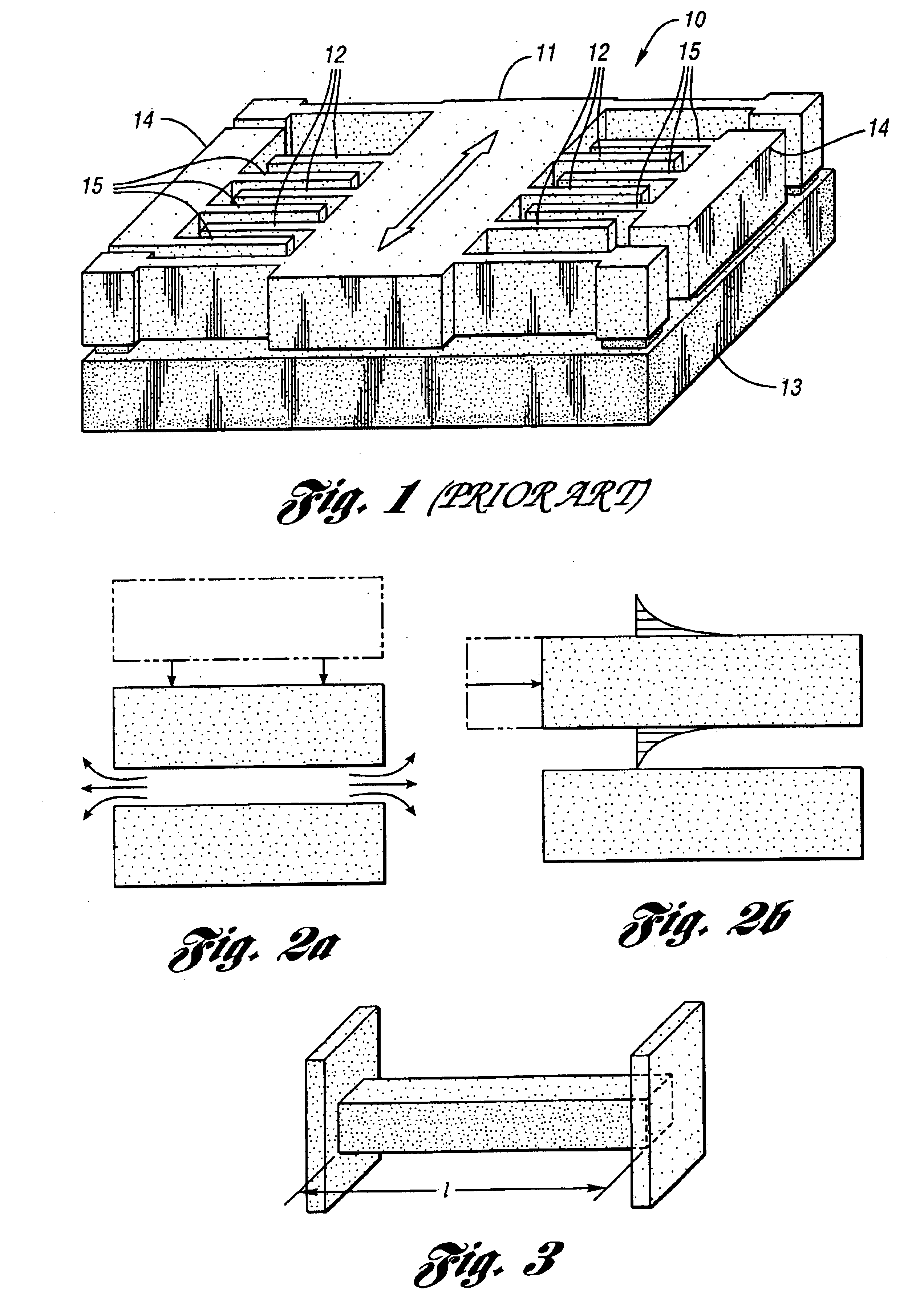
a capacitive lateral accelerometer and micromachined technology, applied in the direction of acceleration measurement in multiple dimensions, acceleration measurement using interia forces, instruments, etc., can solve the problem of low ratio of sensing gap and height of sense electrodes of lateral devices, cantilever-type configuration does not provide adequate stiffness, and has not been implemented with lateral devices.

Inactive Publication Date: 2005-09-06
MICHIGAN UNIV OF RGT
View PDF8 Cites 49 Cited by
  • Summary
  • Abstract
  • Description
  • Claims
  • Application Information

AI Technical Summary

Benefits of technology

[0061]An object of the present invention is to provide a micromachined capacitive lateral accelerometer de

Problems solved by technology

However, the cantilever-type configuration does not provide adequate stiffness if the proofmass is heavy such that it requires a large force to move, which is the case for a high performance device.
It has not been implemented with lateral devices due to relatively small proofmass of the devices and inherent fabrication properties of planar semiconductor process technology.
Since the devices have a very small proofmass, they have suffered from Brownian noise, which is created by random motion of gas molecules, such that it is necessary to increase the mass of the structure in order to achieve high performance devices.
However, the ratio of the sensing gap and the height of sense electrodes of the lateral devices is still relatively small (20˜35) comparing with that of Z-axis devices (>100) due to limitations of the deep RIE technology.
With defining the sensing gap by RIE or deep RIE technology, it is not likely to attain the high-aspect ratio which provides high sensitivity required for high performance accelerometers.
It is desirable to avoid vacuum packaging if possible, since it is not cost effective.
However, from a manufacturing point-of-view, it is not feasible to perforate the plates of in-plane (lateral) devices because the fabrication process of devices has inherent features of a semiconductor technology, so-called planar technology, which is basically to put down and pattern thin films on a substrate.
On the

Method used


Image

  • Micromachined capacitive lateral accelerometer device and monolithic, three-axis accelerometer having same
  • Micromachined capacitive lateral accelerometer device and monolithic, three-axis accelerometer having same
  • Micromachined capacitive lateral accelerometer device and monolithic, three-axis accelerometer having same

Examples


Embodiment Construction

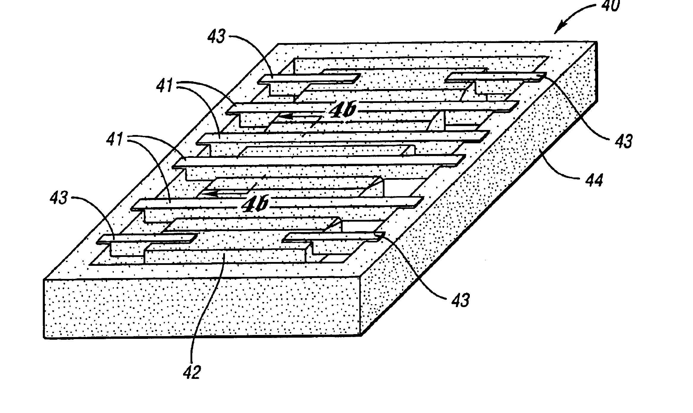
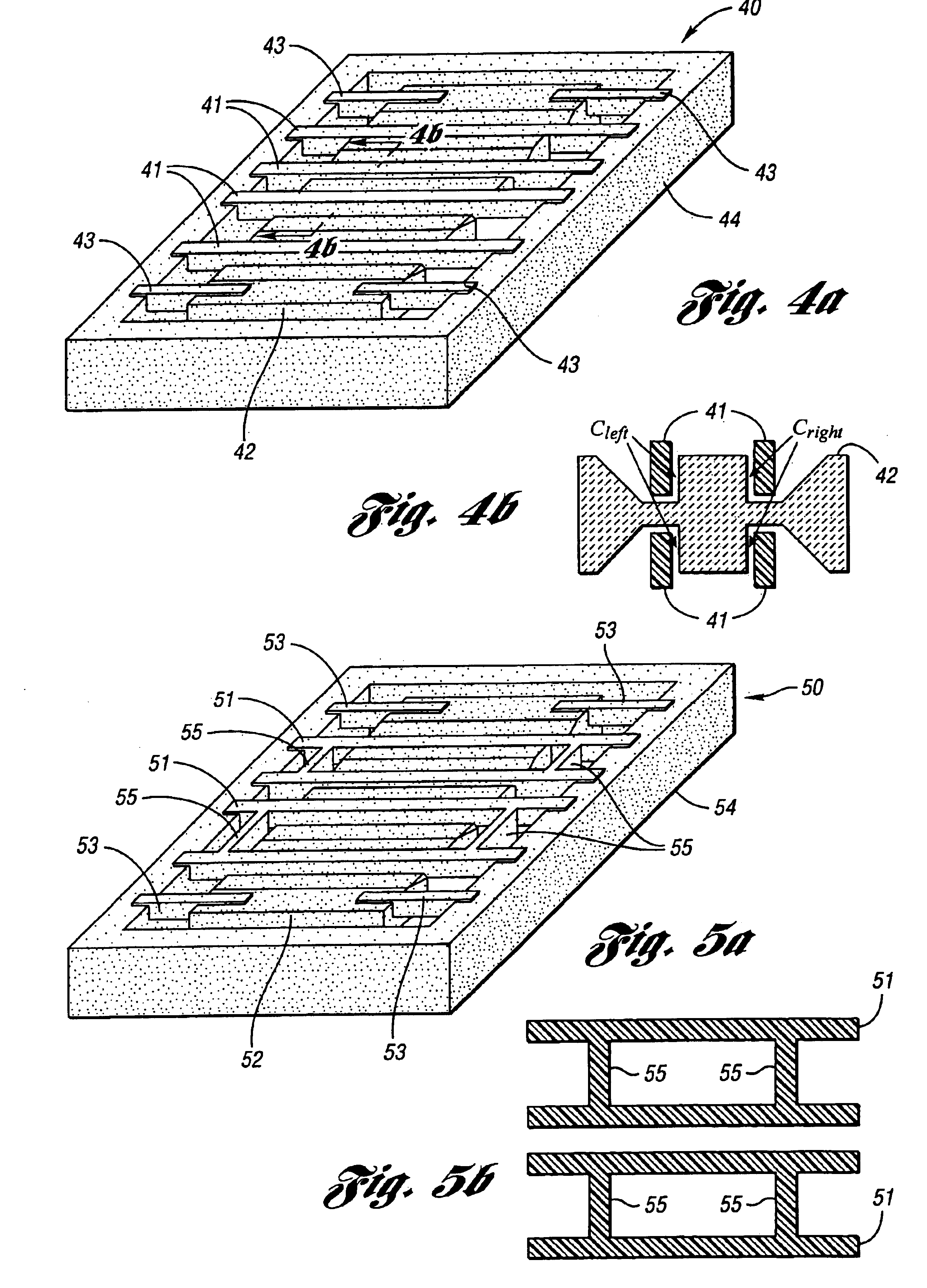
[0111]Briefly, what is disclosed herein is a micromachined in-plane (lateral) accelerometer which utilizes a combined surface and bulk micromachining technology. Several novel features are introduced which are incorporated with a sensor structure as well as approaches to achieve a high-sensitivity, low-noise micromachined accelerometer.

A. In-plane Acceleration Sensor Structure

[0112]a. A new sense and drive electrode configuration[0113]Proofmass itself forms one plate of the parallel-plate capacitor,[0114]Stiff electrodes using a bridge configuration for a stable operation,[0115]b. A novel combined surface and bulk micromachining technology to implement the new sensor structure and electrode configuration[0116]One side of the sense / drive electrode is protected whereas the other side of it is removed at the end of the fabrication using the combined technology,[0117]c. A three-axis single-chip accelerometer[0118]Using the combined technology, a monolithic, three-axis accelerometer was ...


PUM


Abstract

A high-sensitivity and low-noise micromachined capacitive lateral accelerometer device having an input axis and a monolithic, three-axis accelerometer utilizing the device are provided. The device includes at least one electrode having a side surface normal to the input axis. A relatively large proofmass has at least one side surface normal to the input axis and extends along a width of the proofmass. The proofmass is movable against acceleration relative to the at least one electrode due to inertial force along the input axis to obtain a capacitive variation between the at least one electrode and the proofmass. The side surfaces are spaced apart to define a narrow, high-aspect ratio sensing gap which extends along substantially the entire width of the proofmass. The proofmass forms a sense capacitor with the at least one electrode.

Description

CROSS-REFERENCE TO RELATED APPLICATION[0001]This application claims the benefit of U.S. provisional application Ser. No. 60 / 440,567, filed Jan. 16, 2003.STATEMENT REGARDING FEDERALLY SPONSORED RESEARCH OR DEVELOPMENT[0002]This invention was at least partially made with Government support under Contract No. F 30602-98-2-0231, awarded by DARPA. The Government has certain rights in the invention.BACKGROUND OF THE INVENTION[0003]1. Field of the Invention[0004]This invention relates to micromachined capacitive lateral accelerometer devices and monolithic, three-axis accelerometers having such devices.[0005]2. Background Art[0006]The following references are referred to herein by their reference number:[0007][1] Yazdi, N., F. Ayazi, and K. Najafi, “Micromachined Inertial Sensors,” PROCEEDINGS OF THE IEEE, 1998. 86 (8 Aug. 1998): p. 1640-1658.[0008][2] Yazdi, N., “Micro-g Silicon Accelerometers with High Performance CMOS Interface Circuitry, in EECS,” 1999, The University of Michigan: Ann ...

Claims


Application Information

Patent Timeline
IPC IPC(8): G01P15/18G01P15/08G01P15/125B81B3/00
CPCG01P15/0802G01P15/125G01P15/18G01P2015/0814
Inventor NAJAFI, KHALILCHAE, JUNSEOK
Owner MICHIGAN UNIV OF RGT
Why Eureka
Try Eureka