Bipolar transistor and fabrication method thereof

a bipolar transistor and fabrication method technology, applied in the direction of transistors, semiconductor devices, electrical devices, etc., can solve the problems of excessive recombination current generation, deterioration of linearity of current characteristics, and discussion of conventional hbt or sige-bicmos

Inactive Publication Date: 2005-09-06
PANASONIC CORP
View PDF11 Cites 2 Cited by
  • Summary
  • Abstract
  • Description
  • Claims
  • Application Information

AI Technical Summary

Benefits of technology

[0020]Accordingly, the pn junction portion is formed between the emitter diffusion layer including the impurity of the first conductive type at a high concentration and the third semiconductor layer including the impurity of the second conductive type at a high concentration in the upper part of the third semiconductor layer. Hence, the width of the depletion layer formed at the pn junction is narrowed, and a quantity of carriers recombined within the depletion layer is reduced. Consequently, because the recombination current is reduced, the linearity of the current characteristics in a hetero junction type bipolar transistor is improved.
[0026]According to this method, it is possible to control a concentration of the second conductive type impurity doped into the upper part of the third semiconductor layer at a relatively high accuracy by conducting in-situ doping in the third semiconductor layer.
[0028]According to this method, it is possible to dope the second conductive type impurity into the upper part of the third semiconductor layer by relatively simple steps.

Problems solved by technology

However, the above-discussed conventional HBT or SiGe-BiCMOS has problems as follows.
In short, there is an inconvenience that the linearity of the current characteristics is deteriorated in the low bias region of the HBT.
It is assumed that such an excessive recombination current is generated because a depletion layer at the pn junction region in the Si layer is not formed in a satisfactory shape.

Method used


Image

  • Bipolar transistor and fabrication method thereof
  • Bipolar transistor and fabrication method thereof
  • Bipolar transistor and fabrication method thereof

Examples


first embodiment

(First Embodiment)

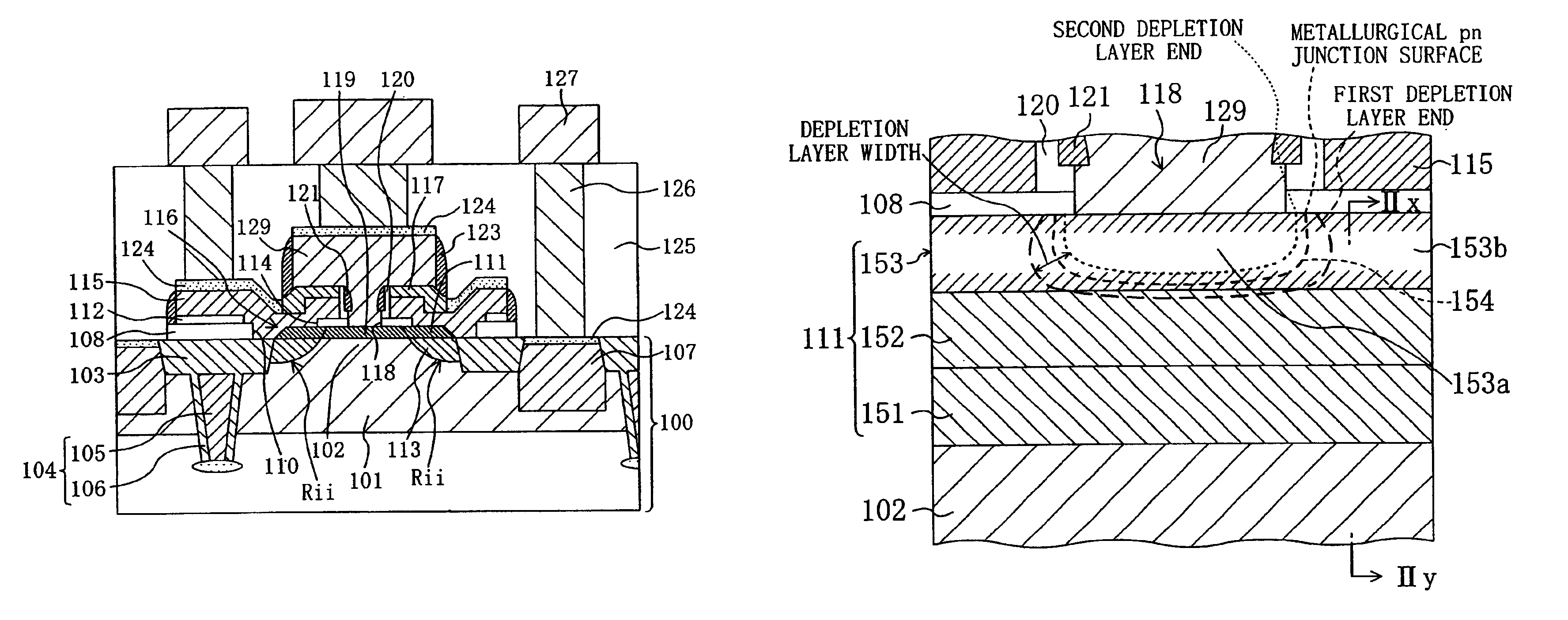
[0061]Initially, the following description will describe, with reference to FIGS. 3(a) through 6(b), a basic flow of the fabrication sequence of an HBT according to a first embodiment.

[0062]Firstly, in the step shown in FIG. 3(a), an N-type retrograde well 101 with a depth of approximately 1 μm is formed on the top portion of an Si substrate 100 having a (001) plane by conducting epitaxial growth of an Si single crystal layer while doping an N-type impurity, or conducting high-energy ion implantation after the epitaxial growth. It should be appreciated, however, that the retrograde well 101 may be formed by conducting ion implantation at a part of the Si substrate 100 without the epitaxial growth. At this point, a region in the vicinity of the surface of the Si substrate 100 is arranged to have a concentration of the N-type impurity at approximately 1×10¹⁷ atoms·cm−3, so that the area will serve as a collector layer of an HBT.

[0063]Then, for the isolation, provided...

second embodiment

(Second Embodiment)

[0085]In the present embodiment, the basic flow of the fabrication sequence of an HBT is the same as described in the first embodiment with reference to FIGS. 2(a) through 6(b).

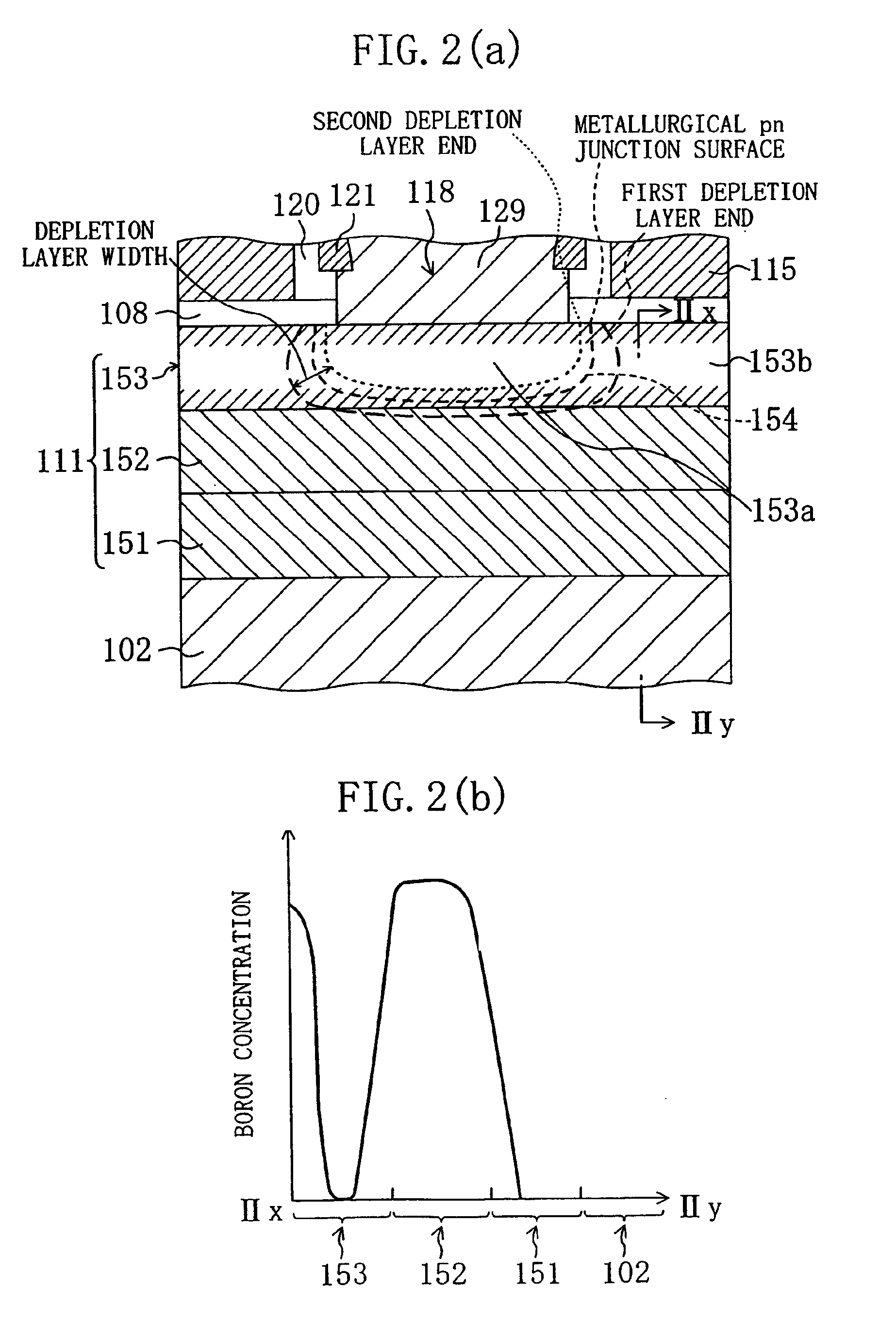
[0086]The present embodiment is characterized in that the step shown in FIG. 4(a) is carried on as described below. FIGS. 8(a) and 8(b) are an enlarged partial cross section showing an emitter-base junction in the step shown in FIG. 4(a) during the fabrication sequence discussed above, and a doping profile of boron along the cross section, respectively.

[0087]In the present embodiment, the treatment is applied in the same manner as was discussed in the first embodiment, whereby formed on the collector layer 102 are an undoped SiGe spacer layer 151 with a thickness of approximately 40 nm and a graded SiGe base layer 152 including boron at a concentration of approximately 4×10¹⁸ atoms·cm−3 with a thickness of approximately 40 nm.

[0088]Then, a supply of hydrogen-diluted diborane (B2H6) is stopp...

third embodiment

(Third Embodiment)

[0094]In the present embodiment, the basic flow of the fabrication sequence of an HBT is the same as described in the first embodiment with reference to FIGS. 2(a) through 6(b).

[0095]The present embodiment is characterized in that the steps shown in FIGS. 4(a) and 4(b) are conducted as described below. FIGS. 9(a) and 9(b) are an enlarged partial cross section showing an emitter-base junction in the steps shown in FIGS. 4(a) and 4(b) during the fabrication sequence discussed above, and a doping profile of boron along the cross section, respectively.

[0096]In the present embodiment, the treatment is applied in the same manner as was discussed in the first embodiment, whereby formed on the collector layer 102 are an undoped SiGe spacer layer 151 with a thickness of approximately 40 nm and a graded SiGe base layer 152 including boron at a concentration of approximately 4×10¹⁸ atoms·cm−3 with a thickness of approximately 40 nm.

[0097]Then, a supply of hydrogen-diluted dib...


PUM


Abstract

A SiGe spacer layer 151, a graded SiGe base layer 152 including boron, and an Si-cap layer 153 are sequentially grown through epitaxial growth over a collector layer 102 on an Si substrate. A second deposited oxide film 112 having a base opening portion 118 and a P+ polysilicon layer 115 that will be made into an emitter connecting electrode filling the base opening portion are formed on the Si-cap layer 153, and an emitter diffusion layer 153a is formed by diffusing phosphorus into the Si-cap layer 153. When the Si-cap layer 153 is grown, by allowing the Si-cap layer 153 to include boron only at the upper part thereof by in-situ doping, the width of a depletion layer 154 is narrowed and a recombination current is reduced, thereby making it possible to improve the linearity of the current characteristics.

Description

[0001]This application is a Div of Ser. No. 10 / 031,445, filed Jan. 22, 2002, now U.S. Pat. No. 6,828,602, which is a 371 of PCT / JP01 / 04344, filed, May 23, 2001.TECHNICAL FIELD[0002]The present invention relates to a hetero junction type bipolar transistor and a fabrication method thereof, and more particularly to a measure to improve a linearity of current characteristics.BACKGROUND ART[0003]Recently, the development has been advancing at a high pitch for a hetero bipolar transistor (HBT) that realizes an operation at a high frequency region with better conduction characteristics conferred by incorporating a hetero junction structure, such as Si / SiGe and Si / SiC, into a bipolar transistor fabricated on a silicon substrate. The HBT uses an Si / SiGe hetero junction structure obtained by allowing epitaxial growth of an SiGe layer on an Si substrate, so that it realizes a transistor operating at a high frequency region at which a conventional transistor cannot operate unless it uses a com...

Claims


Application Information

Patent Timeline
Patent Type & Authority Patents(United States)
IPC IPC(8): H01L29/66H01L21/331H01L21/02H01L29/737H01L29/10H01L29/02H01L29/36H01L29/73H01L29/165
CPCH01L29/1004H01L29/66242H01L29/7378H01L29/36Y10S438/936H01L27/082
Inventor ASAI, AKIRAOHNISHI, TERUHITOTAKAGI, TAKESHI
Owner PANASONIC CORP
Why Eureka
Try Eureka