Method for fabricating semiconductor device having gate electrode with polymetal structure of polycrystalline silicon film and metal film

a technology of polymetal structure and gate electrode, which is applied in the direction of semiconductor devices, basic electric elements, electrical equipment, etc., can solve the problems of difficult application of tungsten silicide to the cmos circuit having the dual gates, and the inability to achieve high-performance circuits in memory devices by using current dual-gate logic devices, etc., to achieve the effect of suppressing the depletion of the gate electrod

Inactive Publication Date: 2005-09-06
TOSHIBA MEMORY CORP
View PDF15 Cites 96 Cited by
  • Summary
  • Abstract
  • Description
  • Claims
  • Application Information

AI Technical Summary

Benefits of technology

[0014]An object of the present invention is to provide a semiconductor device including a polymetal gate structure of the dual gate, which can suppress depletion in the gate electrode of a PMOSFET, and a method for fabricating the same.

Problems solved by technology

Furthermore, diffusivity of dopants in tungsten silicide are several orders of magnitude higher than that in polycrystalline silicon, which has made it difficult to apply tungsten silicide to the CMOS circuits having the dual gates.
However, high-performance circuits cannot be achieved in memory devices by using current dual-gate technology for LOGIC devices because of the poor thermal stability and severe inter-diffusion of gate dopants between P+ gate and N+ gate.
However, the semiconductor device having the polymetal structure fabricating by the above-described fabrication method often has depletion in the gate electrode 104 of the PMOSFET.

Method used


Image

  • Method for fabricating semiconductor device having gate electrode with polymetal structure of polycrystalline silicon film and metal film
  • Method for fabricating semiconductor device having gate electrode with polymetal structure of polycrystalline silicon film and metal film
  • Method for fabricating semiconductor device having gate electrode with polymetal structure of polycrystalline silicon film and metal film

Examples


first embodiment

[0063][A First Embodiment]

[0064]The semiconductor device according to a first embodiment of the present invention and the method for fabricating the semiconductor device will be explained with reference to FIGS. 5, 6A-6D, 7A-7C, 8A-8B and 9A-9B.

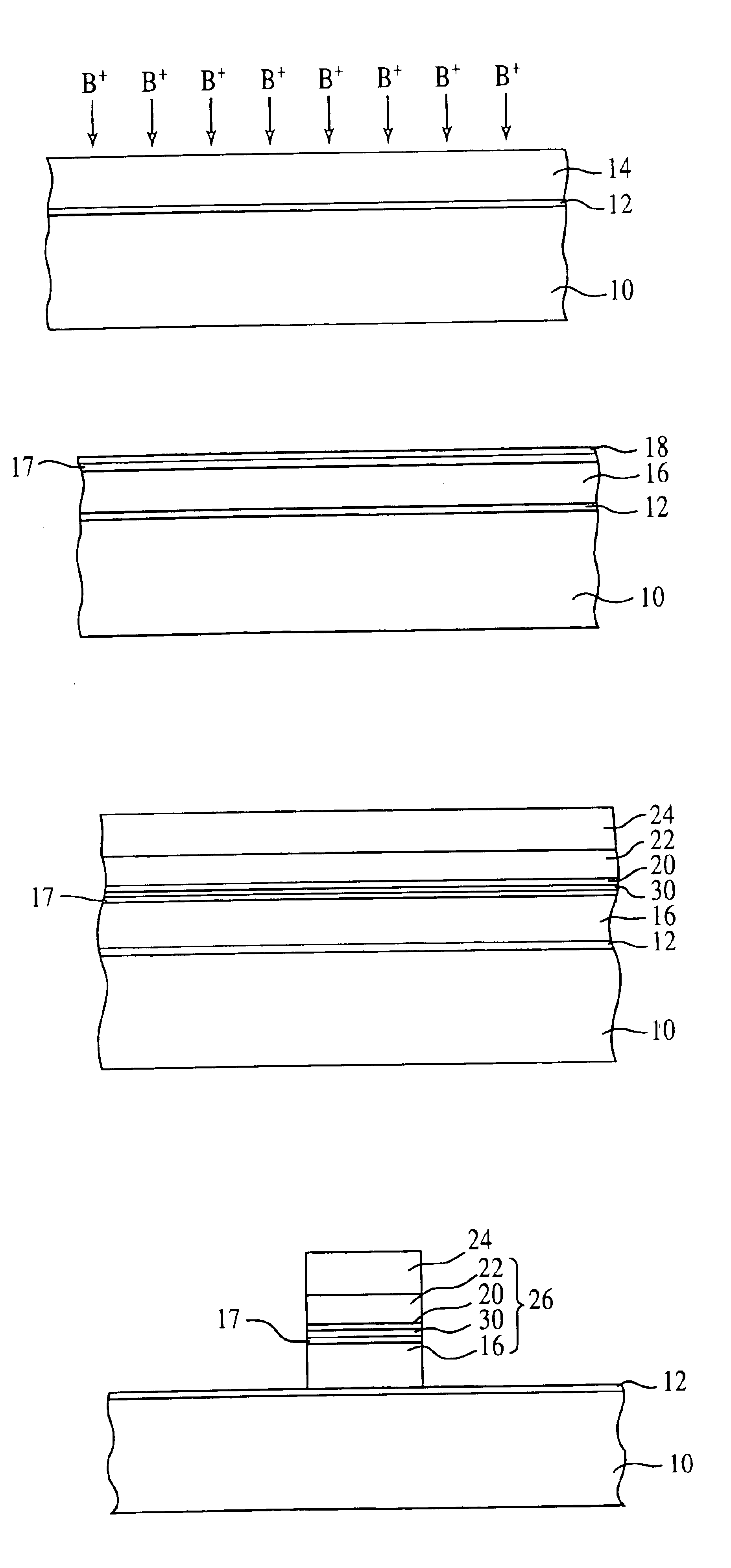
[0065]First, a structure of the semiconductor device according to the present embodiment will be explained with reference to FIG. 5.

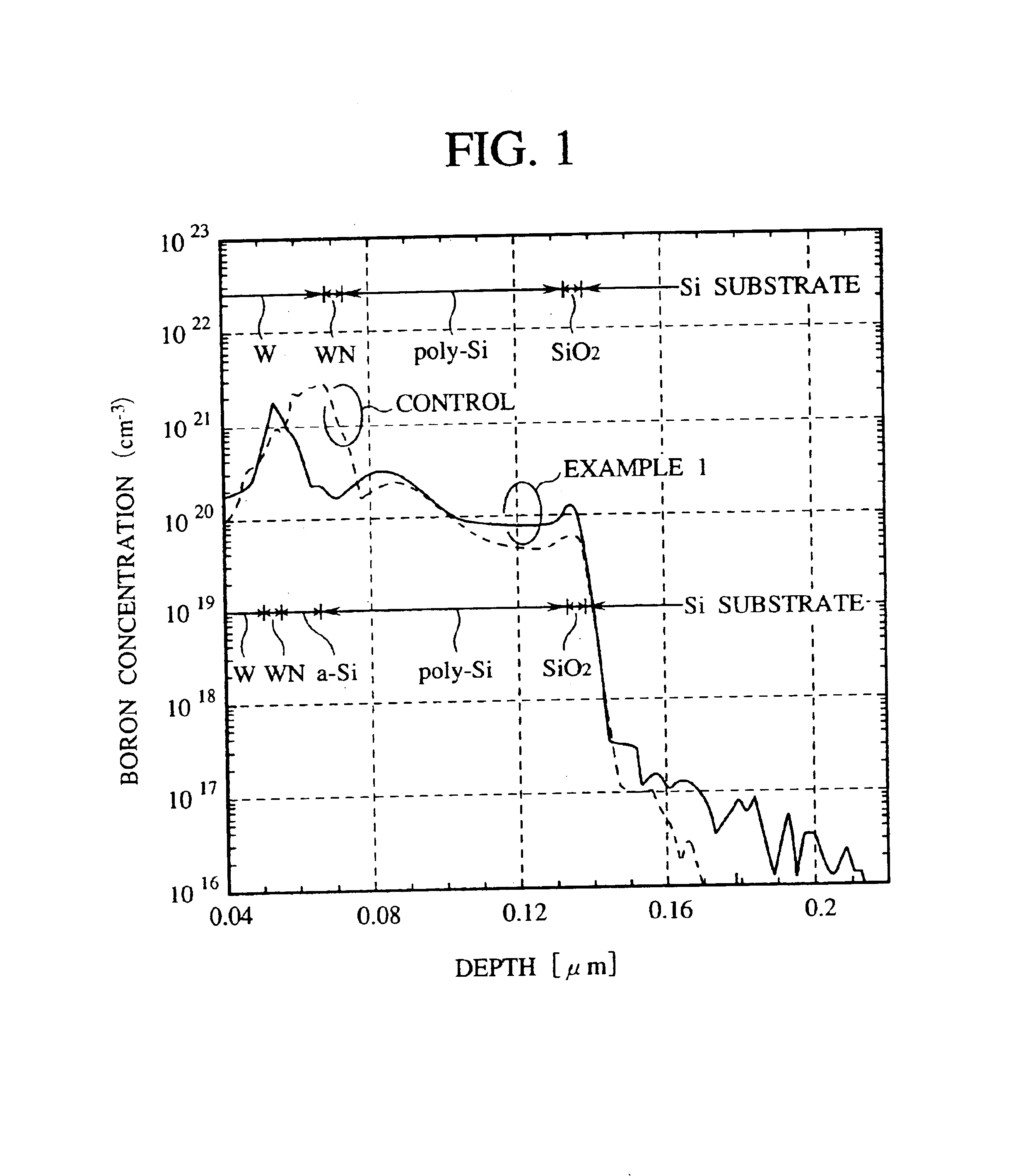
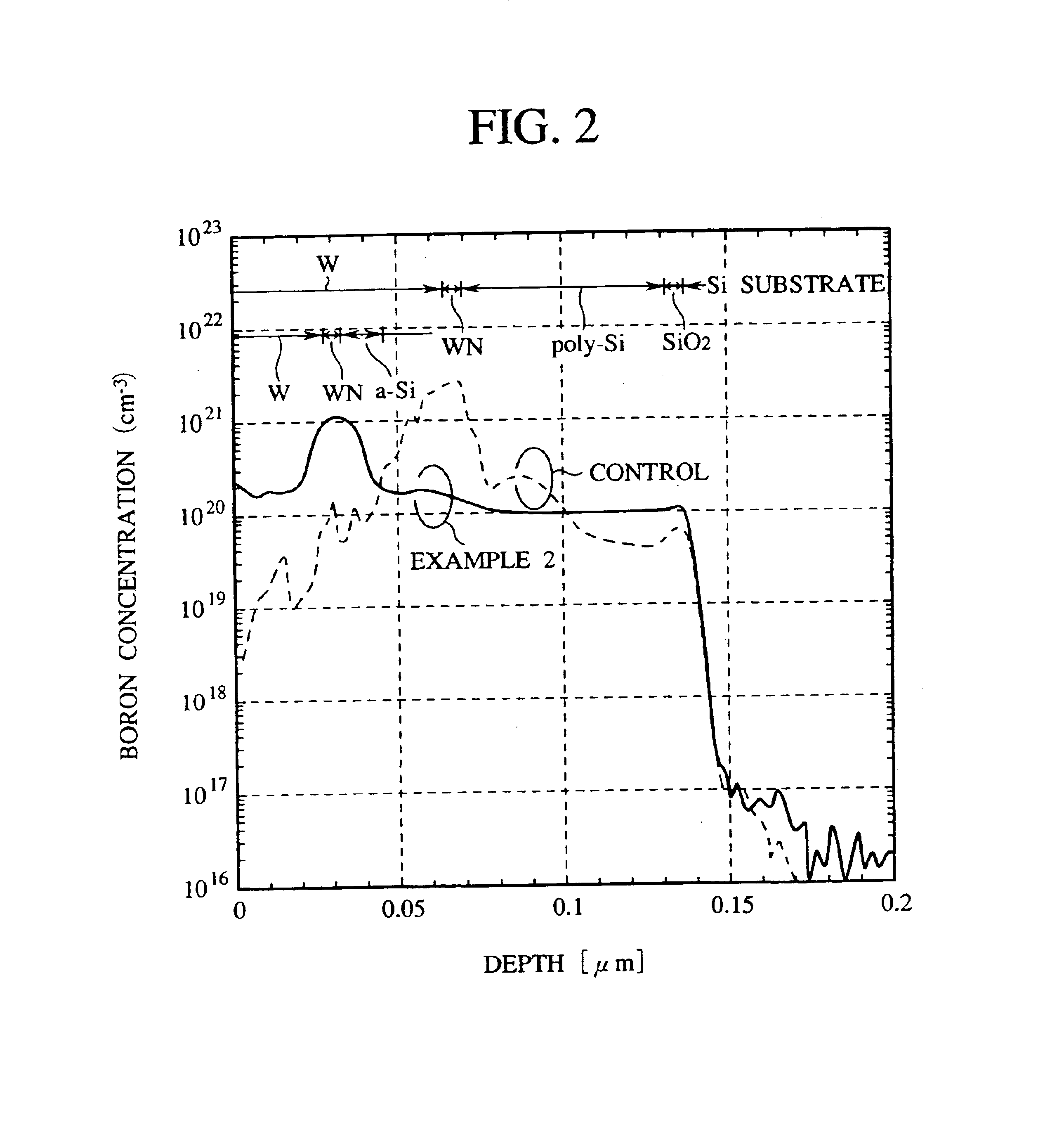
[0066]A gate electrode 26 is formed on a silicon substrate 10 intervening a gate insulation film 12 therebetween. The gate electrode 26 has a layered structure of polycrystalline silicon films 16, 30 formed on the gate insulation film 12, a WN film 20 formed on the polycrystalline silicon film 30, and a W film 22 formed on the WN film 20. The WN film 20 is a barrier metal for preventing the polycrystalline silicon film 30 and the W film 22 from reacting with each other to thereby form tungsten silicide of high resistance. A cap film of a silicon nitride film 24 is formed on the gate electrode 26. A silicon oxide ...

second embodiment

[0086][A Second Embodiment]

[0087]The method for fabricating the semiconductor device according to the second embodiment of the present invention will be explained with reference to FIGS. 10A-10D and 11A-11C. The same members of the semiconductor device according to the first embodiment of the present invention and the method for fabricating the same are represented by the same reference numbers as those of the first embodiment not to repeat or to simplify their explanation. FIGS. 10A-10D and 11A-11C are sectional views of the semiconductor device according to the present embodiment in the steps of the method for fabricating the same, which show the method.

[0088]First, on a silicon substrate 10, a gate insulation film 12 of a 4 nm-thick silicon oxide film containing nitrogen by some percentage is formed by, e.g., thermal oxidation (FIG. 10A).

[0089]Next, a 100 nm-thick polycrystalline silicon film 40 is formed by, e.g., CVD method on the silicon substrate 10 with the gate insulation f...


PUM

PropertyMeasurementUnit
binding energyaaaaaaaaaa
thicknessaaaaaaaaaa
thicknessaaaaaaaaaa

Abstract

The semiconductor device comprises a pair of impurity diffused regions formed in a silicon substrate 10, spaced from each other, and a gate electrode 26 formed above the silicon substrate 10 between the pair of impurity diffused regions 38 intervening a gate insulation film 12 therebetween. The gate electrode 26 is formed of a polycrystalline silicon film 16 formed on the gate insulation film 12, a polycrystalline silicon film 30 formed on the polycrystalline silicon film 16 and having crystal grain boundaries discontinuous to the polycrystalline silicon film 16, a metal nitride film 20 formed on the polycrystalline silicon film 30, and a metal film 22 formed on the barrier metal film 20. Whereby diffusion of the boron from the first polycrystalline silicon film 16 toward the metal nitride film 20 can be decreased. Thus, depletion of the gate electrode 26 can be suppressed.

Description

[0001]This application is a divisional of prior application Ser. No.: 09 / 749,590 filed Dec. 28, 2000 now abandoned, the benefit of which is claimed under 35 U.S.C. §120.BACKGROUND OF THE INVENTION[0002]The present invention relates to a semiconductor device and a method for fabricating the semiconductor device, more specifically to a semiconductor device including gate electrodes of a polymetal structure having laid polycrystalline silicon films and metal films, and a method for fabricating the same.[0003]Conventionally, the gate electrodes of MOSFETs have been formed of single polycrystalline silicon layered structures owing to the thermal stability, the compatibility of polycrystalline silicon with silicon of the substrates in its MOS characteristics, etc. Presently, the so-called polycide structure, which is formed of a silicide film deposited on a polycrystalline silicon film, is dominantly used for the end of decreasing sheet resistance of the gate electrodes while utilizing th...

Claims


Application Information

Patent Timeline
Patent Type & Authority Patents(United States)
IPC IPC(8): H01L21/28H01L21/02H01L29/49H01L29/40H01L29/78
CPCH01L21/28061H01L21/28247H01L29/4941H01L29/6656
Inventor OHTAKE, FUMIOAKASAKA, YASUSHIMURAKOSHI, ATSUSHISUGURO, KYOICHI
Owner TOSHIBA MEMORY CORP
Why Eureka
Try Eureka