

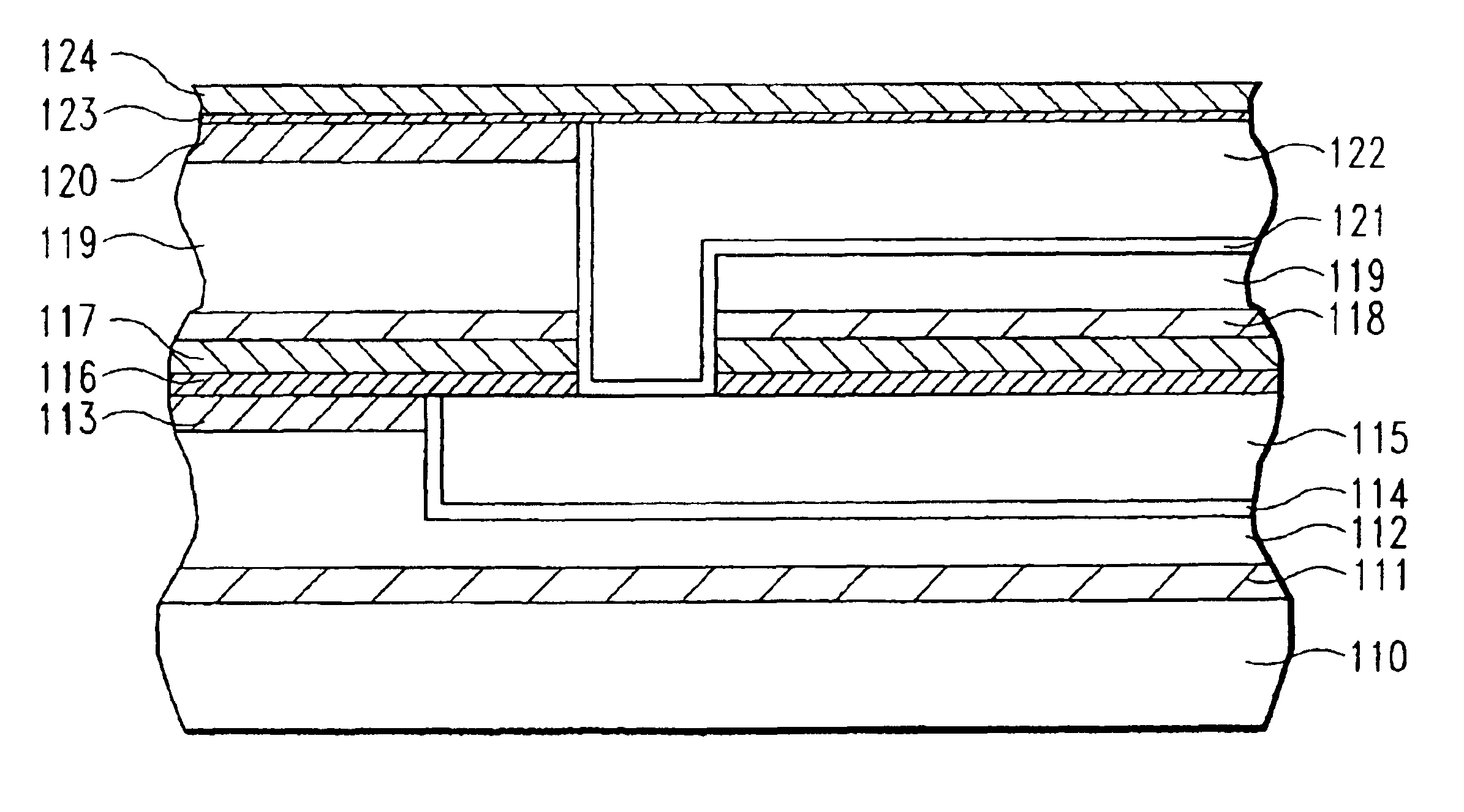
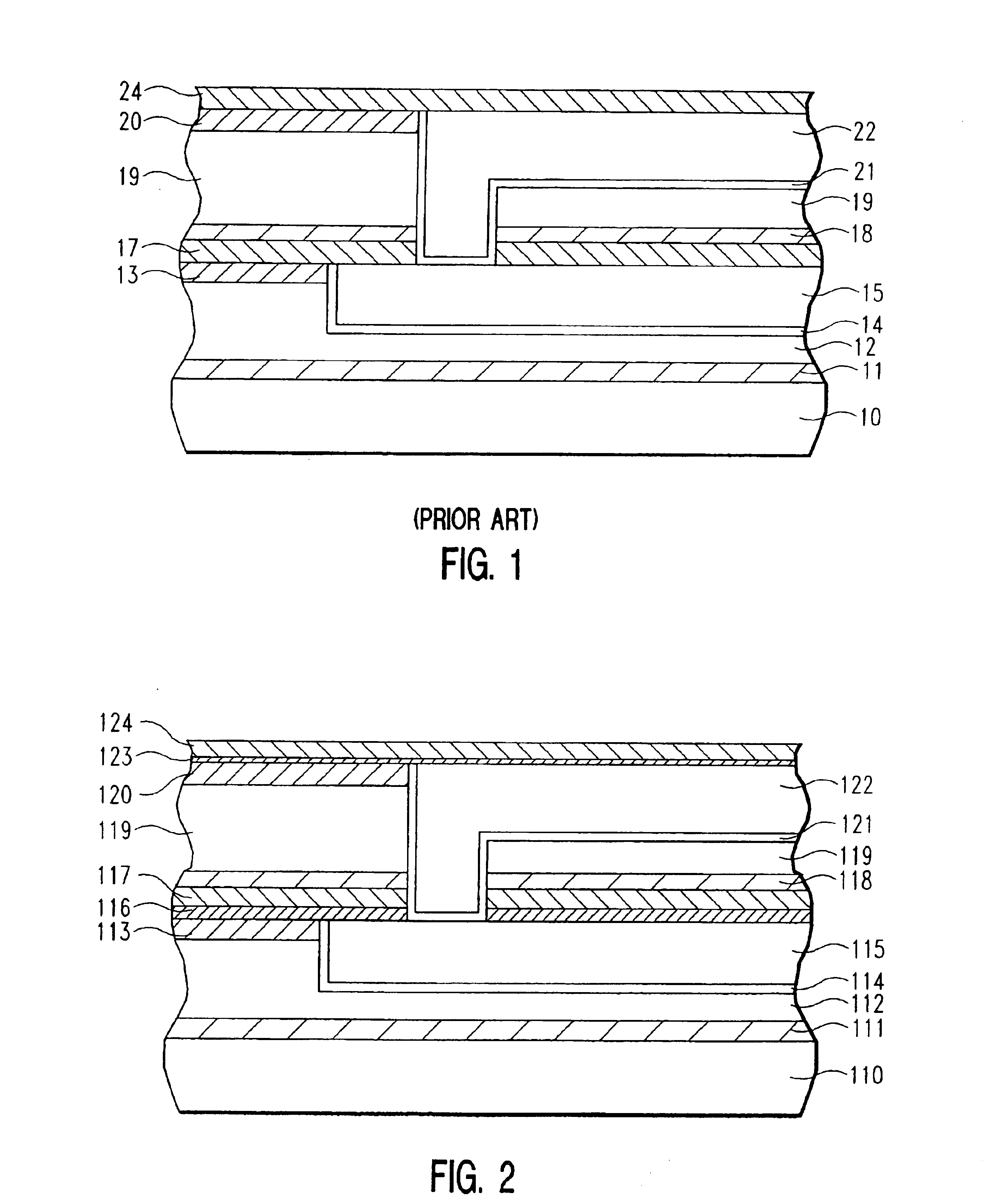
Advanced BEOL interconnect structures with low-k PE CVD cap layer and method thereof
a technology of backend of line and cvd cap layer, which is applied in the direction of semiconductor devices, semiconductor/solid-state device details, electrical apparatus, etc., can solve the problems of poor adhesion of silicon nitride films deposited using conventional pe cvd processes, copper suffers from an important disadvantage, and the effect of plasma-enhanced chemical vapor deposition
- Summary
- Abstract
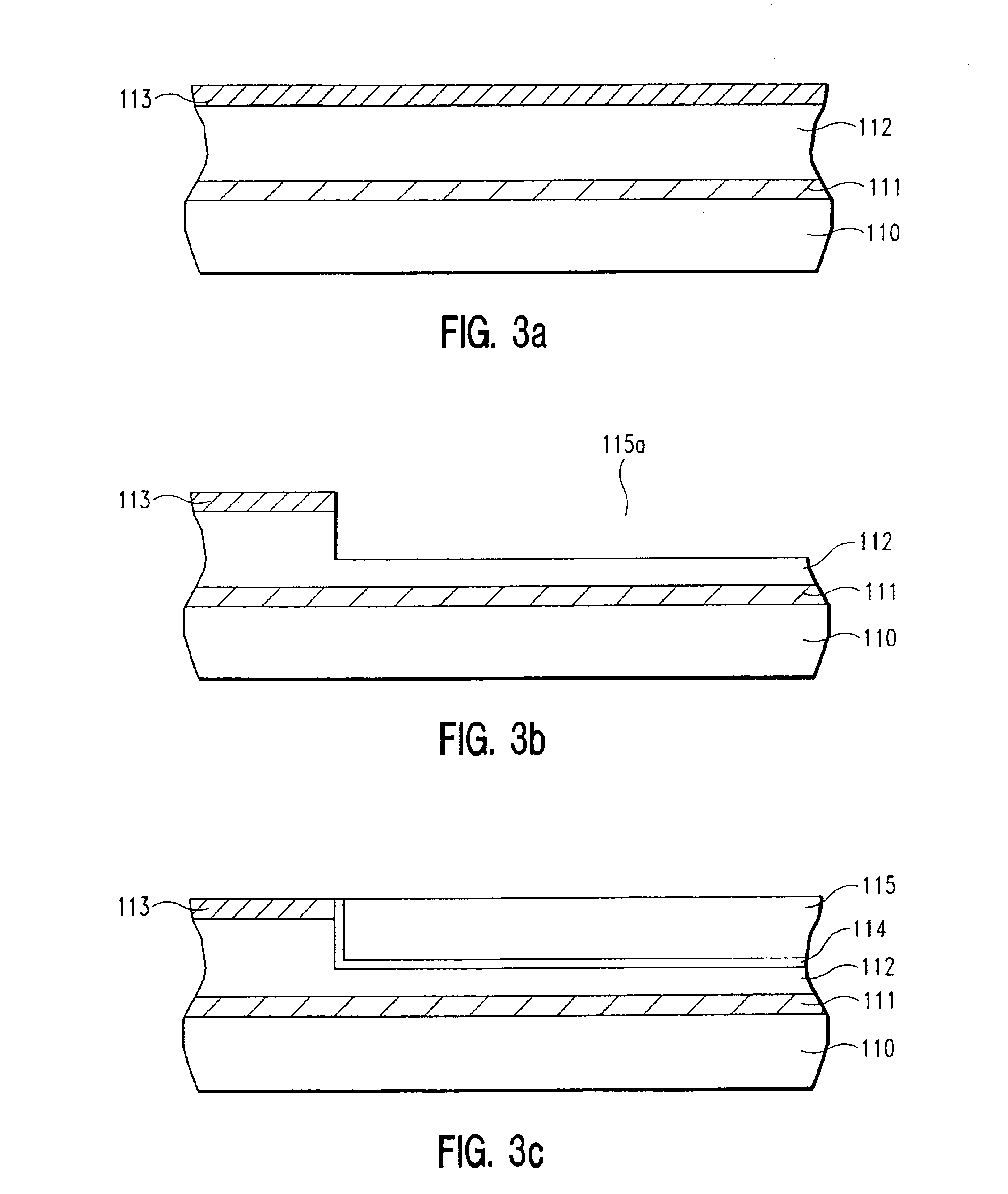
- Description
- Claims
- Application Information
AI Technical Summary
Benefits of technology
Problems solved by technology
Method used
Image

Examples
example 1
[0057]A series of semiconductor wafers containing partially fabricated interconnect structures were prepared, each comprising a plurality of copper conductors embedded in SiLK™ low-k dielectric material. The wafers each had been planarized in a CMP step such that the top surface of the copper conductors was made coplanar with the surface of a hardmask layer overlying the low-k dielectric material. Each wafer was subjected to a different pre-clean step, in which the high frequency RF power, low frequency RF power, flow rate of NH3, and flow rate of N2 were varied. The time of exposure during each pre-clean step was 18 seconds. The high frequency RF power (HF RF), low frequency RF power (LF RF), NH3 flow rate and N2 flow rate for each pre-clean step are listed in Table 1.
[0058]
TABLE 1Pre-clean Exposure VariablesN2WaferHF RF (W)LF RF (W)NH3 (sccm)(sccm)Adhesion13501004000030.0290450270080011.332503001200100017.542503001200016.651653001200100011.061655001200100010.271153001200100011.083...
example 2
[0061]Two semiconductor wafers containing partially fabricated interconnect structures were prepared, each comprising a plurality of copper conductors embedded in SiLK™ low-k dielectric material. The wafers each had been planarized in a CMP step such that the top surface of the copper conductors was made coplanar with the surface of a hardmask layer overlying the low-k dielectric material.
[0062]Each wafer was subjected to a different pre-clean step, in which the high frequency RF power, low frequency RF power, and flow rate of NH3 were kept constant, but the sequence of pre-clean and deposition steps was varied. For each wafer, the high frequency RF power was 350 watts, the low frequency RF power was 100 watts, and the flow rate of NH3 was 4000 sccm. The pre-clean exposure time for each wafer was 18 seconds. Following pre-clean, a silicon nitride cap layer was deposited on each wafer. For the first wafer, a single pre-clean step was performed, and then the silicon nitride cap layer ...
PUM
| Property | Measurement | Unit |
|---|---|---|
| pressure | aaaaa | aaaaa |
| pressure | aaaaa | aaaaa |
| pressure | aaaaa | aaaaa |
Abstract
Description
Claims
Application Information