Multi-column charged particle optics assembly

a technology of charged particles and optics, applied in the field of electron optic structures, can solve the problems of inability to use in-line in semiconductor fabrication facilities, the resolution requirements of defect inspection tools become more demanding, and the limited resolution of the problem of assembly, so as to facilitate the manufacture of the assembly

Inactive Publication Date: 2005-09-13
TOKYO ELECTRON LTD +1
View PDF31 Cites 43 Cited by
  • Summary
  • Abstract
  • Description
  • Claims
  • Application Information

AI Technical Summary

Benefits of technology

[0008]The present invention provides a multi-column charged particle optics assembly for incorporation in various inspection, imaging and analytical systems. The multi-column optics assembly comprises at least one optical component which is continuous through the entire optics assembly, all other optical components are one per column and are independently alignable to the optical axes of their corresponding columns. Examples of optical components which can be continuous through the entire optics assembly are the accelerator structure (which includes the first accelerator electrode and the final accelerator electrode), the focus electrode mounting plate and the gun mounting plate. These continuous components can provide mechanical integrity to the electron optics assembly and facilitate the manufacture of the assembly.

Problems solved by technology

The systems used for inspection typically use light optics and such systems are limited in resolution due to the wavelength of the measuring light (200-400 nm).
As the feature sizes on semiconductor wafers drop below 0.18 μm, the resolution requirements of the defect inspection tools become more demanding.
These systems have been effective for research and product development, but are impractical for use in-line in a semiconductor fabrication facility.
Multiple columns built on a single wafer must be “perfect” columns as-fabricated, since there is no facility for adjusting the physical electron optical alignment of any column; further, the electron optical components of the column are restricted to what can be fabricated on a semiconductor wafer.
The cluster of physically separate electron beam columns is costly to manufacture.

Method used


Image

  • Multi-column charged particle optics assembly
  • Multi-column charged particle optics assembly
  • Multi-column charged particle optics assembly

Examples


Embodiment Construction

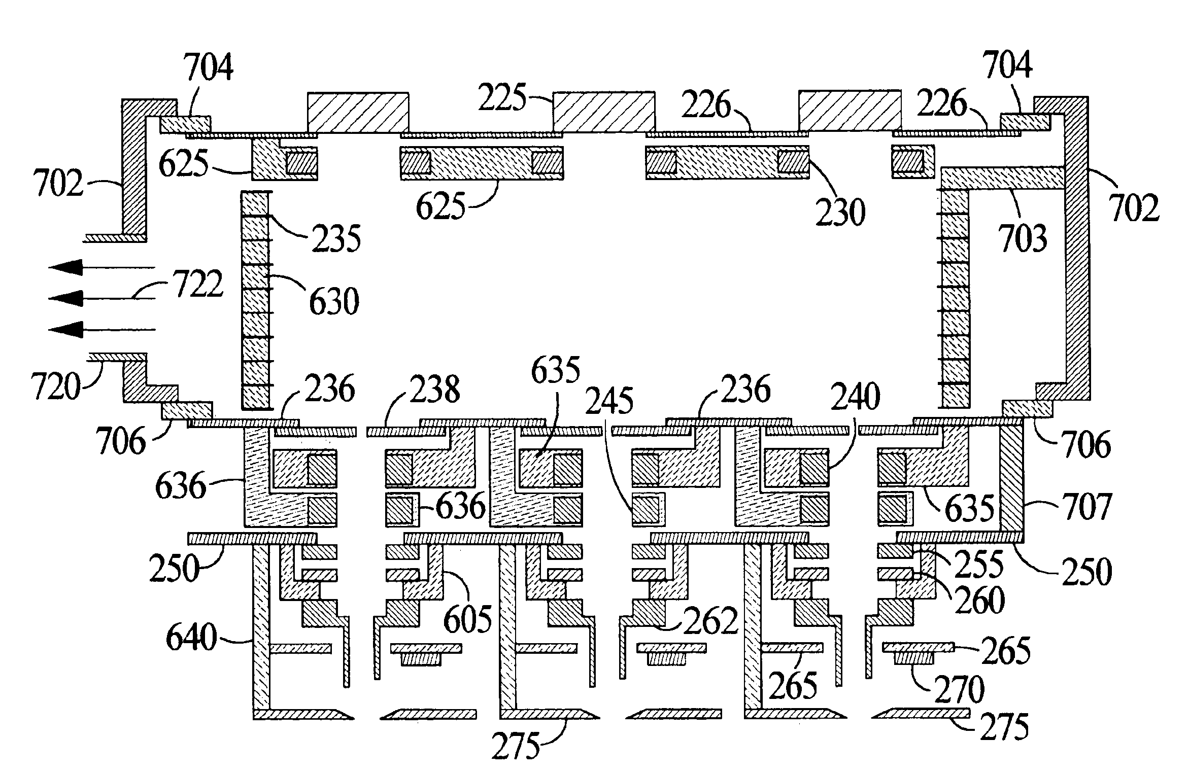
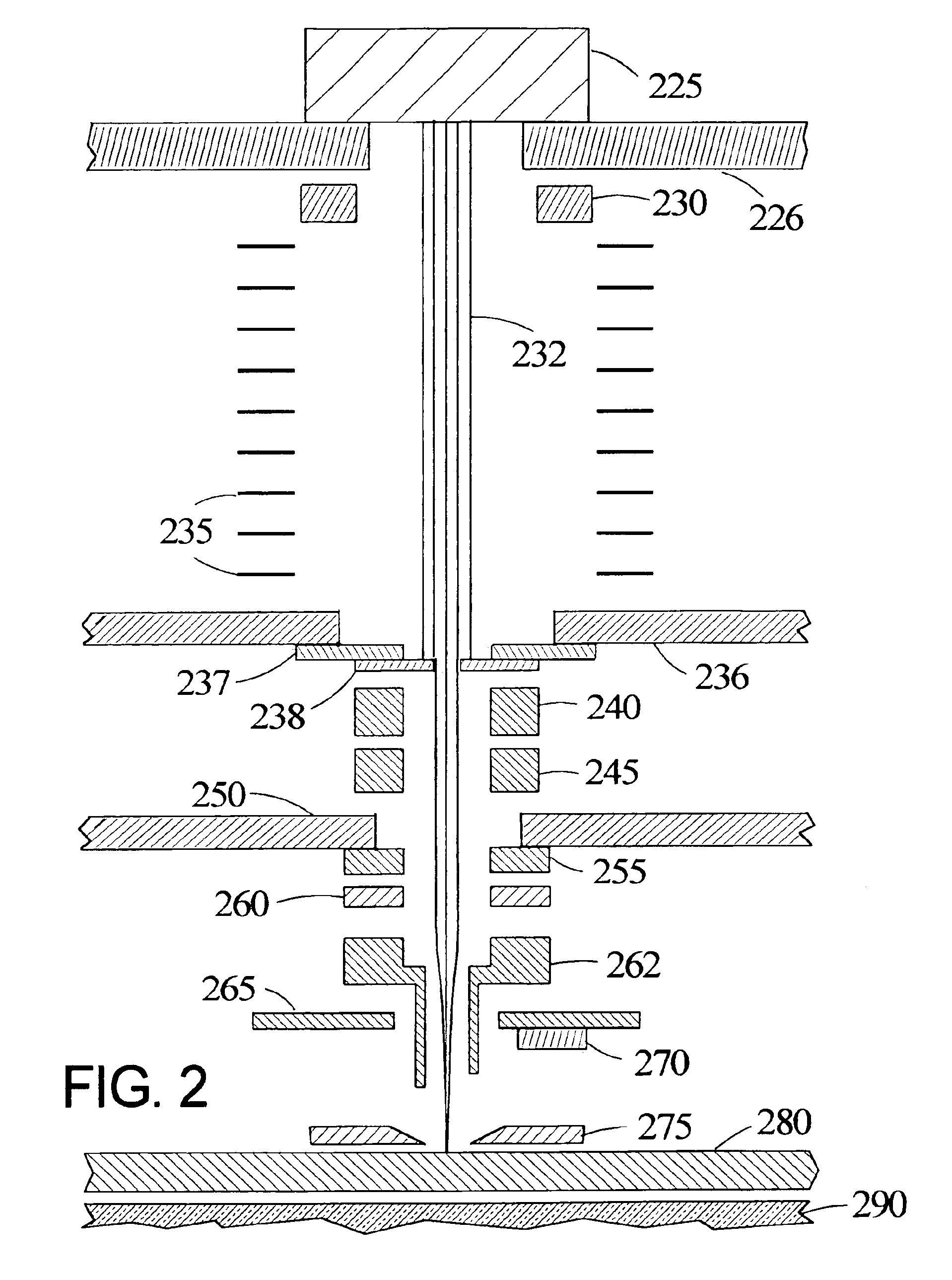
[0024]The invention disclosed herein is a multiple column charged particle optical assembly. The assembly can be optimized for use with either ion or electron beams. The optical components of the assembly can be fabricated on a millimeter scale, and are consequently well suited for millimeter scale charged particle beam columns (typically comprised of electrostatic lenses, stigmators, deflectors, etc.). Such an assembly comprising millimeter scale columns can constitute the imaging part of a multi-beam multi-column electron beam inspection system for the semiconductor industry (where multiple columns must fit over a semiconductor wafer or mask). The multiple columns allow for high throughput substrate inspection. Certain embodiments of this invention are designed for the detection of defects for features with critical dimensions (CDs) in the range 25 nm-100 nm, with a substrate throughput suitable for in-line use in a semiconductor fabrication facility.

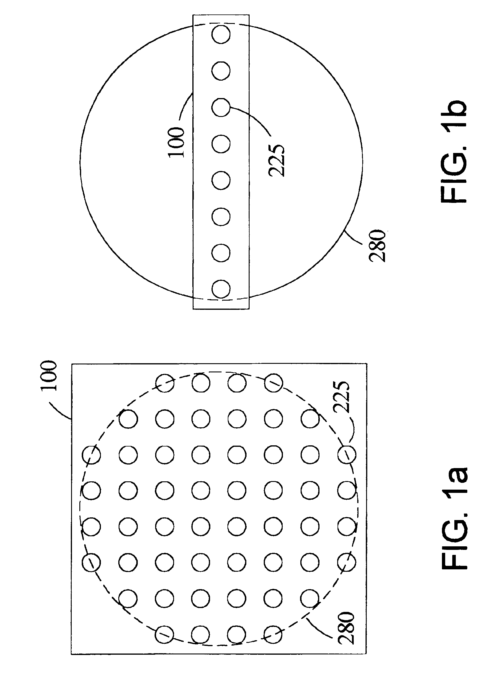
[0025]FIG. 1a shows a schemati...


PUM

PropertyMeasurementUnit
wavelengthaaaaaaaaaa
sizesaaaaaaaaaa
diameteraaaaaaaaaa

Abstract

A multi-column charged particle optics assembly comprises: a first optical component which is continuous through all columns of the charged particle optics assembly; and a multiplicity of independently alignable second optical components coupled to the first optical component, such that there is one second component for each column in the charged particles optics assembly. The first component provides mechanical integrity to the charged particle optics assembly and each second optical component is independently alignable to the optic axis of its corresponding column. In a further embodiment, the charged particle optics assembly comprises: first and second continuous optical components; and a multiplicity of independently alignable electrodes coupled to the second optical component, such that there is a corresponding independently alignable electrode for each column.

Description

CROSS-REFERENCE TO RELATED APPLICATIONS[0001]This application is a continuation-in-part of U.S. application Ser. No. 10 / 222,759 filed Aug. 15, 2002, now U.S. Pat. No. 6,734,428, which is a continuation-in-part of U.S. application Ser. No. 09 / 789,180 filed Feb. 19, 2001, now abandoned which in turn claims the benefit of U.S. Provisional Application No. 60 / 183,724 filed Feb. 19, 2000.BACKGROUND OF THE INVENTION[0002]1. Field of the Invention[0003]This invention relates to the field of charged particle optics, and in particular to electron optical structures used for wafer inspection.[0004]2. Description of the Related Art[0005]Defect inspection of semiconductor wafers and masks for IC manufacturing is an accepted production process for yield enhancement. The information obtained from a wafer defect inspection tool can be used to flag defective wafers for reprocessing, or to correct wafer processing parameters. The systems used for inspection typically use light optics and such systems...

Claims


Application Information

Patent Timeline
Patent Type & Authority Patents(United States)
IPC IPC(8): G01N23/00G21K7/00H01J37/08G21K5/10H01J37/30G01Q20/02G01Q30/02H01J37/065
CPCH01J37/065H01J37/32862H01J2237/0635H01J2237/1501H01J2237/2817
Inventor PARKER, N. WILLIAMMILLER, S. DANIELGALANDE, VICTOR A.
Owner TOKYO ELECTRON LTD
Why Eureka
Try Eureka