This helps you quickly interpret patents by identifying the three key elements:
Problems solved by technology
Method used
Benefits of technology
Benefits of technology
[0017]It is another object of the invention to provide a light emitting diode which can exhibit desired performance in a light source size substantially equal to the size of the light emitting element and can enhance phosphor excitation efficiency.
[0024]The conductive layer may be formed of a p electrode. In this case, the p electrode can have both a light reflecting function and a wire bonding function. The formation of the p electrode on the whole surface of a p-type layer in the light emitting element can improve reflection efficiency and, at the same time, can render wire bonding easier. Further, unlike the prior art technique, there is no need to additionally provide a pad electrode for wire bonding, and wire bonding directly to the p electrode is possible. This can simplify the production process.
[0030]According to this construction, a part of phosphor-originated light can be obtained by the phosphor contained in the mount. Therefore, a light source capable of emitting a desired color and having a size substantially equal to the size of the light emitting element can be provided without increasing the concentration of the phosphor in the phosphor-mixed layer to such a level that causes absorption and attenuation of the light emitted from the light emitting element. Thus, a light emitting diode can be realized in which the light source size is substantially equal to the size of the light emitting element and, at the same time, the efficiency of giving off fluorescence upon excitation can be enhanced.
[0031]In the invention, when a construction is adopted wherein the light emitting diode is used as a light source and a reflector is provided opposite to the light emitting element, since a light source size substantially equal to the size of the light emitting element is possible, the quantity of light, which is reflected from a portion around the center of the reflector and is blocked by the light source, is very small. Further, no light is reflected obliquely from the reflector, and the light can be reflected substantially parallel to the central axis of the reflector. Therefore, a reflection light emitting diode can be realized in which the efficiency of radiating light to the outside of the light emitting diode is high, light distribution can also be regulated, and light can be radiated substantially parallel to the central axis of the reflector.
Problems solved by technology
A large number of emission colors, particularly a large number of emission colors with broad-band emission spectrum cannot be realized by light emission inherent in active semiconductor materials in inorganic light emitting elements, or can be realized only with low efficiency.
Due to these facts, the quantity of yellow light emitted is unsatisfactory.
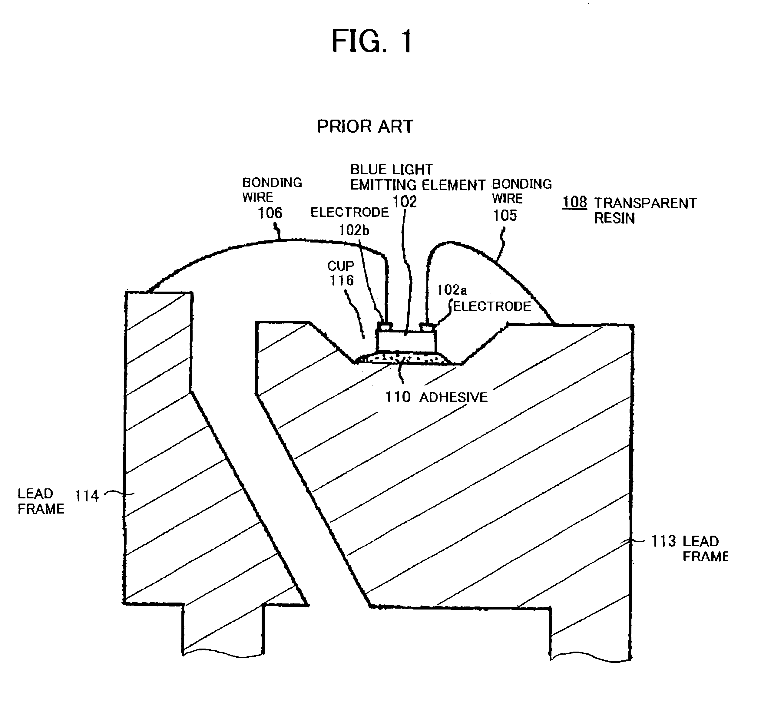
Thus, the light emitting diode shown in FIG. 1 is disadvantageous in that a desired color such as white color cannot be uniformly emitted from the whole light radiating surface of the light emitting diode.
Therefore, the size of the light source is large, and this large light source size poses various problems.
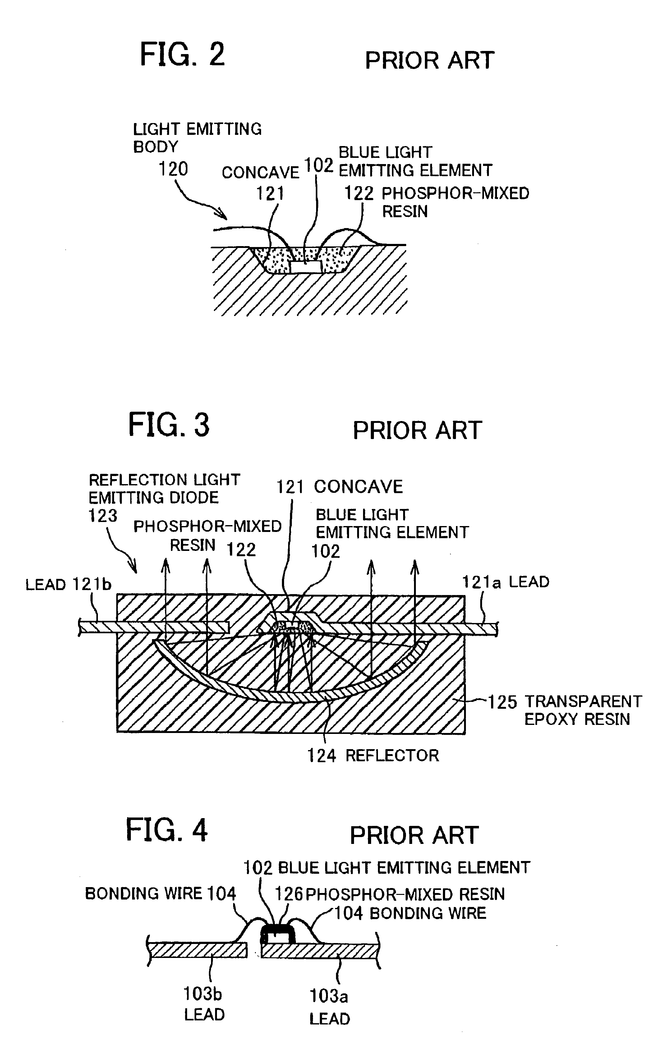
However, this cannot be achieved by the following problems: (i) the size of the concave 121 constituting the light source is so large that light reflected from a portion around the center of the reflector 124 is blocked by the concave 121 and cannot be radiated outside the light emitting diode; and (ii) since the diameter of the light source is large, the light beam is spread and consequently is disadvantageously reflected obliquely from the reflector 124 and cannot be radiated in a substantially perpendicular direction.
Further, the reflection light emitting diode shown in FIGS. 2 and 3 has an additional problem (iii) that, because of the large original light source, white light, which has been radiated outside the light emitting diode, cannot be focused to a small size by a focusing optical system.
This disadvantageously poses a problem of low fluorescence excitation efficiency.
Method used
Image
Click on the blue label to locate the original text in one second.
Reading with bidirectional positioning of images and text.
Examples
first preferred embodiment
(First Preferred Embodiment)
[0050]FIG. 5 is a cross-sectional view showing the construction of the so-called “lens-type light emitting diode” in the first preferred embodiment of the invention. This light emitting diode includes a blue light emitting element 4 and lead frames 1, 2. A metal stem 3 provided with a cup 10 is extended from the lead frame 1. The blue light emitting element 4 is formed of a GaN-base semiconductor and is located in the cup 10 and is mounted on the metal stem 3 through a mount 5. The cup 10 functions as a reflector which reflects light emitted from the blue light emitting element 4 above the light emitting diode.
[0051]The p electrode 48 is a light nontransparent, light reflective, thick conductive metal layer. The p electrode 48 is electrically connected to the lead frame 1 through a gold bonding wire 6, and the n electrode 49 is electrically connected to the lead frame 2 through a gold bonding wire 7. The metal stem 3 and the lead frame 1 are often collect...
second preferred embodiment
(Second Preferred Embodiment)
[0065]A light emitting diode in a second preferred embodiment of the invention will be explained in conjunction with FIG. 7. In FIGS. 7 and 5, like parts are identified with the same reference characters, and the overlapped explanation thereof will be omitted.
[0066]The light emitting diode shown in FIG. 7 is of SMD (surface mounted device) type and has the following construction. Two leads 14, 15, which are formed of a gold pattern and are electrically insulated from each other, are provided on the upper and lower sides of an insulating glass-epoxy resin board 12. A frame 17 provided with a plastic cup 17a is provided on the leads 14, 15. The inner surface of the cup 17a functions as a reflector which reflects light emitted from the blue light emitting element 4. The leads 14, 15 are asymmetrical with respect to each other. The upper surface of the lead 15 extends to the center portion of the bottom of a space provided by the cup 17a in the frame 17. On ...
third preferred embodiment
(Third Preferred Embodiment)
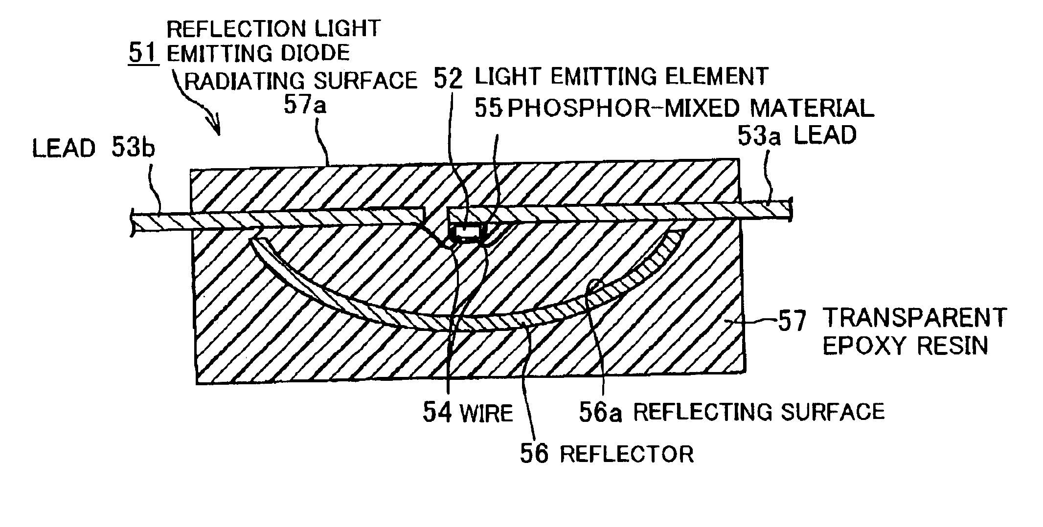
[0073]The light emitting diode in the third preferred embodiment of the invention will be explained in conjunction with FIGS. 8, 9, 10, 11A, and 11B.
[0074]At the outset, a light source part of a reflection light emitting diode in the third preferred embodiment of the invention will be explained in conjunction with FIG. 8. As shown in FIG. 8, the light source part of the reflection light emitting diode in the third preferred embodiment includes a blue light emitting element (hereinafter referred to simply as “light emitting element”) 52. A pair of leads 53a, 53b are provided for supplying electric power to the light emitting element 52. The light emitting element 52 is mounted onto the leading end of the lead 53a. In this case, a mount paste 55a with a phosphor incorporated therein is interposed between the light emitting element 52 and the lead 53a. A phosphor-mixed material 55 is also coated onto the upper surface and side face of the light emitting elem...
PUM
Abstract
In a light emitting diode, a blue light emitting element is mounted on a base having a cup through a phosphor-containing mount so that the light emitting element is located within the cup and is mounted on the bottom of the cup through the phosphor-containing mount. The light emitting diode includes a light emitting element and a p electrode. By virtue of the above construction, blue light emitted from the light emitting element can be reflected from the lower surface of the p electrode without being radiated directly from the upper surface of the light emitting element to the outside of the light emitting diode. As a result, the blue light emitted from the light emitting element can be efficiently mixed with yellow light given off from the phosphor in the phosphor-containing mount to provide white light which is radiated to the outside of the light emitting diode with high efficiency. The white light can be perceived by a viewer to be uniformly radiated from the light radiating surface of the light emitting diode.
Description
[0001]The present application is based on Japanese Patent Applications No. 2002-102665 and No. 2002-244303, the entire contents of which are incorporated herein by reference.BACKGROUND OF THE INVENTION[0002]1. Field of the Invention[0003]The invention relates to a light emitting diode including a light emitting element and a phosphor. More particularly, the invention is concerned with a light emitting diode including a light emitting element and a phosphor in which light of a predetermined color emitted from the light emitting element is mixed with photoluminescence given off from the phosphor to provide light having a mixed color which is then radiated to the outside of the light emitting diode. In this specification, an LED chip per se is referred to as “light emitting element,” and the whole system including an LED chip-mounted package resin or lens system or other optical system is referred to as “light emitting diode.”[0004]2. Related Art[0005]Light emitting elements, which are...
Claims
Application Information
Patent Timeline
Application Date:The date an application was filed.
Publication Date:The date a patent or application was officially published.
First Publication Date:The earliest publication date of a patent with the same application number.
Issue Date:Publication date of the patent grant document.
PCT Entry Date:The Entry date of PCT National Phase.
Estimated Expiry Date:The statutory expiry date of a patent right according to the Patent Law, and it is the longest term of protection that the patent right can achieve without the termination of the patent right due to other reasons(Term extension factor has been taken into account ).
Invalid Date:Actual expiry date is based on effective date or publication date of legal transaction data of invalid patent.

