DC-coupled multi-stage amplifier using all-pass resistive/capacitive network for level shifting

a level shifting and amplifier technology, applied in the field of high-frequency amplifiers, can solve the problems of high cost of broadband resonance-free inductors, difficult cascading amplifier stages, and incompatibility of bias point (4v) of drain of first amplifier stage with bias point (0.3v) of second amplifier stag

Inactive Publication Date: 2005-09-13
AGILENT TECH INC
View PDF3 Cites 45 Cited by
  • Summary
  • Abstract
  • Description
  • Claims
  • Application Information

AI Technical Summary

Problems solved by technology

However, cascading amplifier stages can be difficult due to the incompatibility of the bias levels of the output of one amplifier stage with the input of the next amplifier stage.
The output signal is coupled to the input of the next amplifier stage; however, the bias point (4V) of the drain of the first amplifier stage is not compatible with the bias point (−0.3V) of the second amplifier stage.
Similarly, the inductor 22 often has resonant frequencies that affect the signal between amplifier stages, and broadband resonance-free inductors are expensive.
Higher operating temperatures often result in earlier failures, especially with physically small resistors.
Unfortunately, physically large resistors do not work well at high frequencies due to parasitic reactance.

Method used


Image

  • DC-coupled multi-stage amplifier using all-pass resistive/capacitive network for level shifting
  • DC-coupled multi-stage amplifier using all-pass resistive/capacitive network for level shifting
  • DC-coupled multi-stage amplifier using all-pass resistive/capacitive network for level shifting

Examples


Embodiment Construction

I. Introduction

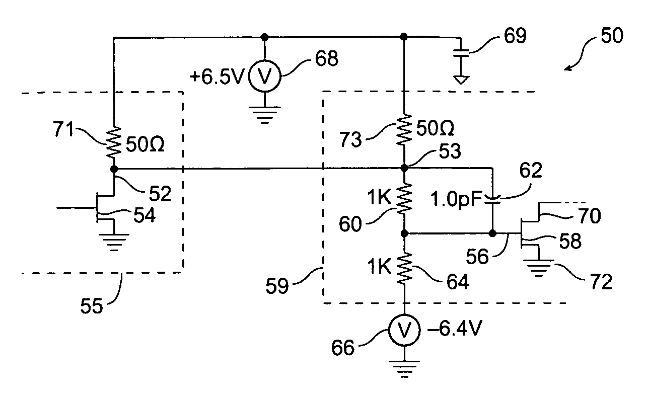
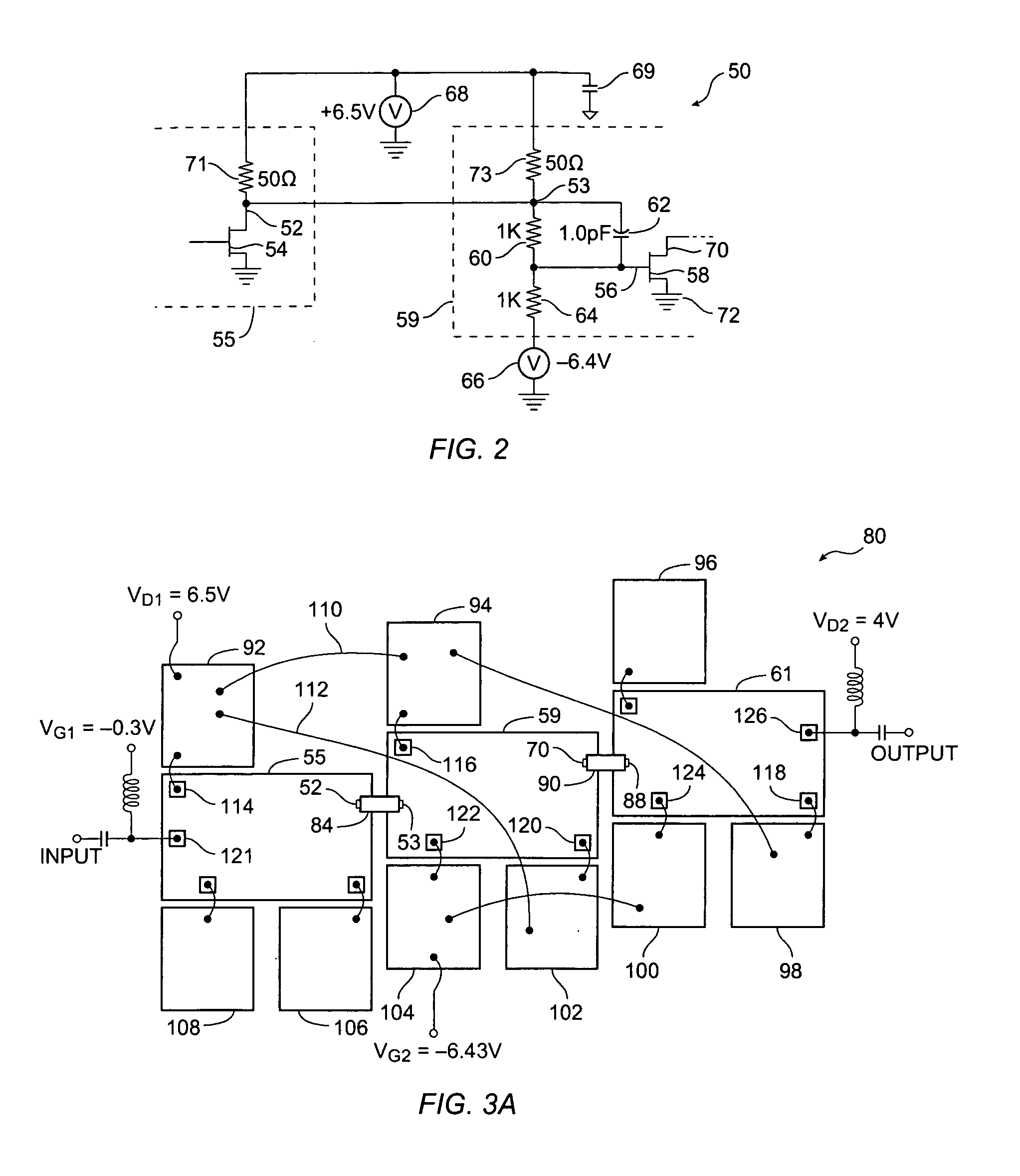
[0028]Cascaded amplifier stages are DC-coupled in a multi-stage amplifier. Bias current to a first amplifier stage is provided through both the output termination resistor of the first amplifier stage and the input termination resistor of the following amplifier stage. Thus, in a 50-ohm system, drain current for the first amplifier stage is provided through 25 ohms, which is the parallel combination of a 50 ohm output termination of the first amplifier stage and the 50 ohm input termination of the following amplifier stage. This results in lower power dissipation than providing bias current through only the output termination resistor. Resistors and a capacitor integrated on the amplifier chip provide a level-shifting network to bias a gate of the following amplifier stage and to couple the output of the first amplifier stage to the gate of the following amplifier stage from DC to several GHz.

II. Exemplary Multi-Stage Amplifier

[0029]FIG. 2 is a simplified circuit diag...


PUM


Abstract

A resistive level-shifting biasing network is used with a capacitor in parallel to couple FET-based amplifier stages from DC to several GHz in a multi-stage amplifier. The output of the first amplifier stage is connected to the input of the second amplifier stage without a blocking capacitor or level-shifting diodes, allowing a portion of the drain current for the first amplifier stage to be supplied from the second amplifier stage. In a particular embodiment, a distributed amplifier achieved over 20 dB gain from DC to about 80 GHz using three traveling wave amplifier chips.

Description

CROSS-REFERENCE TO RELATED APPLICATIONS[0001]Not applicable.STATEMENT REGARDING FEDERALLY SPONSORED RESEARCH OR DEVELOPMENT[0002]Not applicable.REFERENCE TO MICROFICHE APPENDIX[0003]Not applicable.FIELD OF THE INVENTION[0004]The present invention relates generally to high-frequency amplifiers, and more particularly to biasing amplifier stages in a multi-stage amplifier using an integrated, resistive level-shifting network.BACKGROUND OF THE INVENTION[0005]Broadband amplification (generally from less than 100 MHz to greater than 75 GHz) is desired for many applications, such as microwave and optical communication networks and test and measurement equipment. Gain of approximately 20–30 dB is desirable to obtain moderate power levels (typically about 10 to 30 dBm) for electrical signals. Distributed amplifier integrated circuits (“ICs”), particularly those using gallium arsenide (“GaAs”) and / or indium phosphide (“InP”) transistors, are often used as gain elements in these types of syste...

Claims


Application Information

Patent Timeline
Patent Type & Authority Patents(United States)
IPC IPC(8): H03F1/30
CPCH03F1/306H03F2200/288
Inventor SCHERRER, DANIEL R.BREITBARTH, JASON R.SCHMELZER, DAVID P.CULVER, MORGAN K.D'AVANZO, JR., DONALD C.
Owner AGILENT TECH INC
Why Eureka
Try Eureka