

Image pickup apparatus having a common amplifier
a pickup apparatus and amplifier technology, applied in the direction of radio frequency control devices, instruments, television systems, etc., can solve the problems of insufficient examination of the scanning circuit for efficiently performing addition/non-addition switching operation, ineffective downsizing, etc., and achieve the effect of reducing the circuit scale of the scanning circui
- Summary
- Abstract
- Description
- Claims
- Application Information
AI Technical Summary
Benefits of technology
Problems solved by technology
Method used
Image

Examples
first embodiment
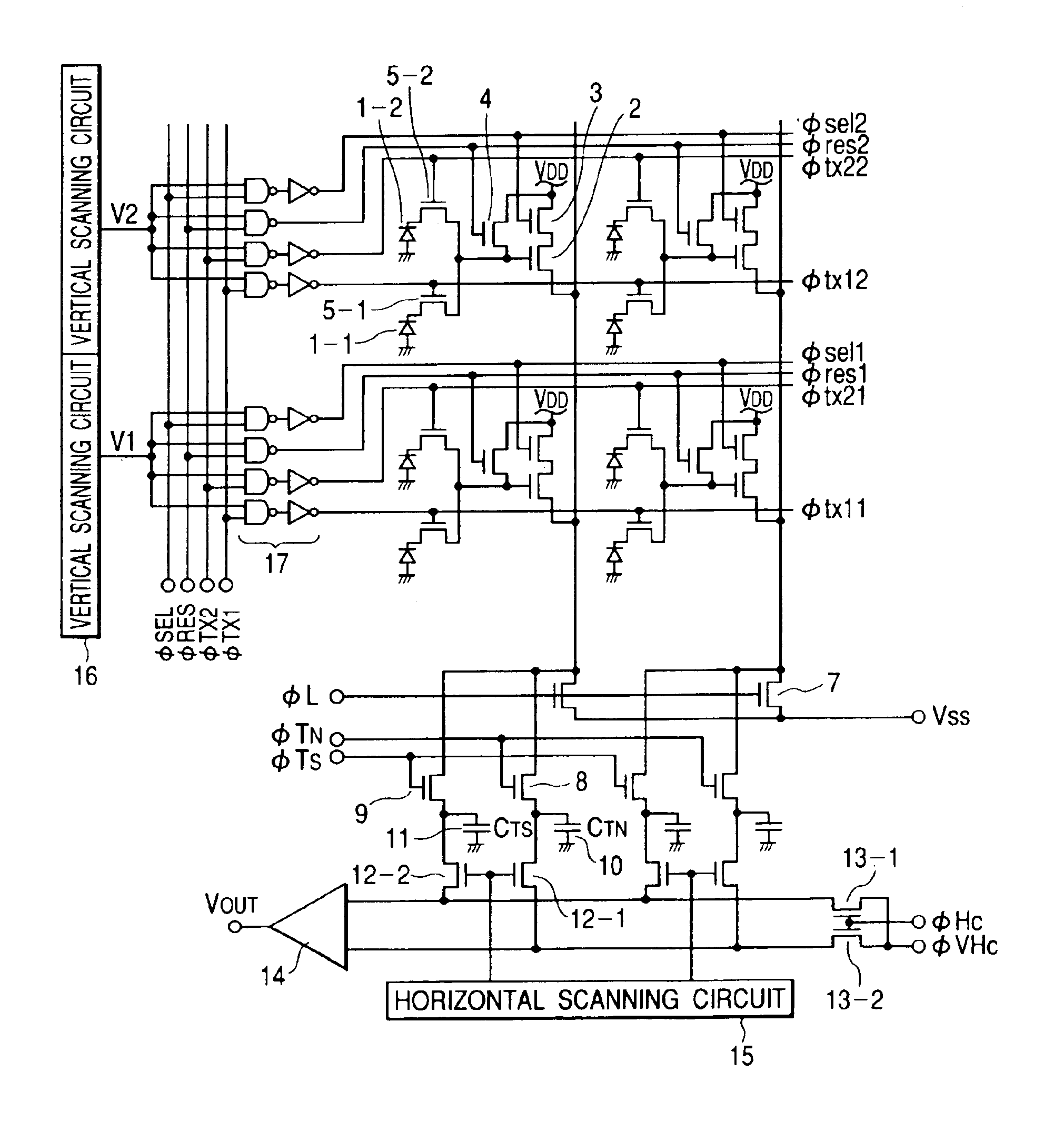
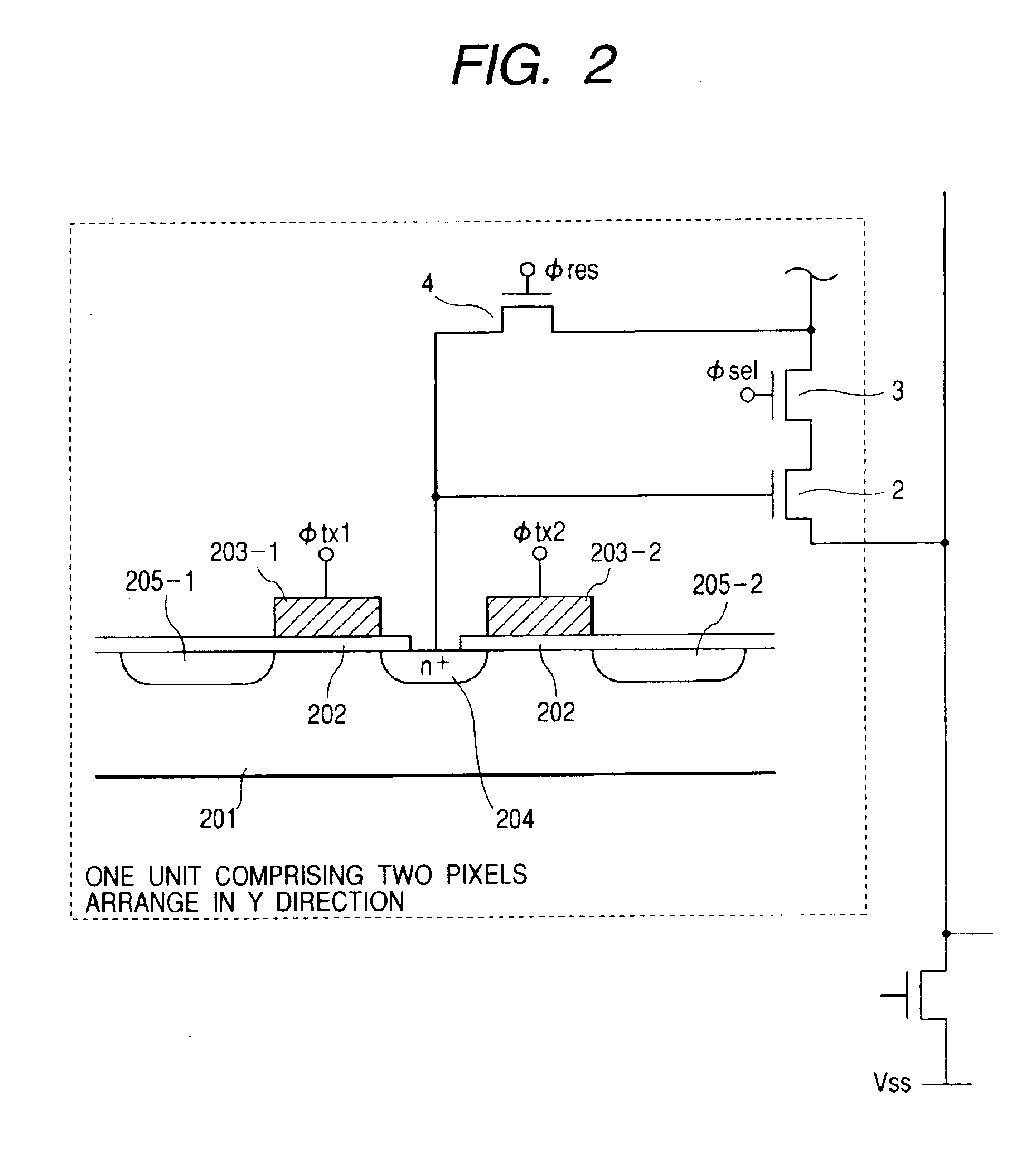
[0030]The first embodiment realizes sensor read operation by generating a vertical scanning timing signal only once while controlling the pixel arrays of the two, first and second lines. Thus, the circuit arrangement of the vertical scanning circuit can be simplified, the vertical scanning circuit can be reduced along with pixel reduction, and a small-size solid-state image pickup element can be implemented.
[0031]In the first embodiment, a pair of circuits for generating the reset clock φres and vertical selection clock φsel necessary for read of each of the first and second lines are arranged for and shared by the two, first and second lines, thereby also reducing the circuit scale.
[0032]Addition and read-out of signals from two pixels at the FD portion 204 can also be realized by changing only the timings of application pulses without changing the circuit arrangement of the first embodiment. FIG. 4 is a timing chart when signals from two, upper and lower pixels are added. The timi...
second embodiment
[0039]Addition and read-out of signals from four pixels in the Y direction at an FD portion 204 can also be easily realized by changing only the timings of application pulses without changing the circuit arrangement of the
[0040]FIG. 6 is a circuit diagram showing the equivalent circuit of a solid-state image pickup element according to the third embodiment of the present invention. In the third embodiment, an arithmetic processing unit 17 is comprised of transfer gates 601 and switch MOS transistors 602. Reference numeral 603 denotes an inverter which generates the inverted signal of a vertical scanning timing clock.
[0041]The operation of the third embodiment will be explained with reference to the timing chart of FIG. 3. Similar to the first embodiment, after photoelectric conversion elements are reset, accumulation operation starts. At the end of the accumulation time, a timing output V1 from a vertical scanning circuit 16 goes high to turn on transfer gates 601-1 to 601-4. Extern...
fourth embodiment
[0046]The fourth embodiment can, therefore, obtain new effects: the number of external clocks can be reduced, the solid-state image pickup element can be easily controlled, and the area for laying out clock wires can be reduced.
[0047]The vertical scanning circuit in each of the first to fourth embodiments may be a shift register circuit or decoder circuit. The shift register circuit can reduce the circuit scale more than the decoder circuit. The decoder circuit can freely select the pixel column selection order and can realize various signal read-out orders in comparison with the shift register circuit.
[0048]As has been described above, the first to fourth embodiments can implement a solid-state image pickup element in which the peripheral circuit is downsized, resulting in low cost by downsizing and high yield, a small-size package, a small-size optical system, and a simple external control circuit.
[0049]FIG. 10 is a schematic view showing an image pickup apparatus such as a digita...
PUM
 Abstract
Description
Claims
Application Information