Wide band electro-optical modulators

a wide band, electro-optical technology, applied in the direction of optics, optical waveguide light guides, instruments, etc., can solve the problems of affecting the quality of transmission, and increasing the power consumption of the modulation frequency with the modulation frequency. achieve the effect of good frequency respons

Inactive Publication Date: 2005-09-20
CENT NAT DE LA RECHERCHE SCI
View PDF7 Cites 4 Cited by
  • Summary
  • Abstract
  • Description
  • Claims
  • Application Information

AI Technical Summary

Benefits of technology

[0018]The aim of the invention is therefore to provide an optical modulator having good frequency response and which eliminates the <<chirp>> phenomenon.

Problems solved by technology

However, their implementation at flow rates as high as 40 Gb / s involves the simultaneous resolution of a number of problems.
These problems are notably those of a flat frequency response of the modulator, its power consumption which increases rapidly with the modulation frequency.
Finally, at flow rates as high as 40 Gb / s, dispersion problems arise, although small when compared to the external modulation of the light—by a modulator—at the direct modulation of a semiconductor laser.
These dispersion problems, with external modulators, for example in lithium niobate, are connected to the ratio between the residual phase modulation and the intensity modulation generated.
This may be detrimental to the quality of a transmission in a dispersive medium and translate in a degradation of the signal shape which jeopardises the reception of a digital signal.
However, it is possible to show that the frequency response of an X-section modulator is less favourable than that of a Z-section modulator.
Moreover, it is very difficult to design and obtain control electronics with a 40 GHz pass-band capable of delivering 12 V peak to peak voltages.

Method used


Image

  • Wide band electro-optical modulators
  • Wide band electro-optical modulators
  • Wide band electro-optical modulators

Examples


Embodiment Construction

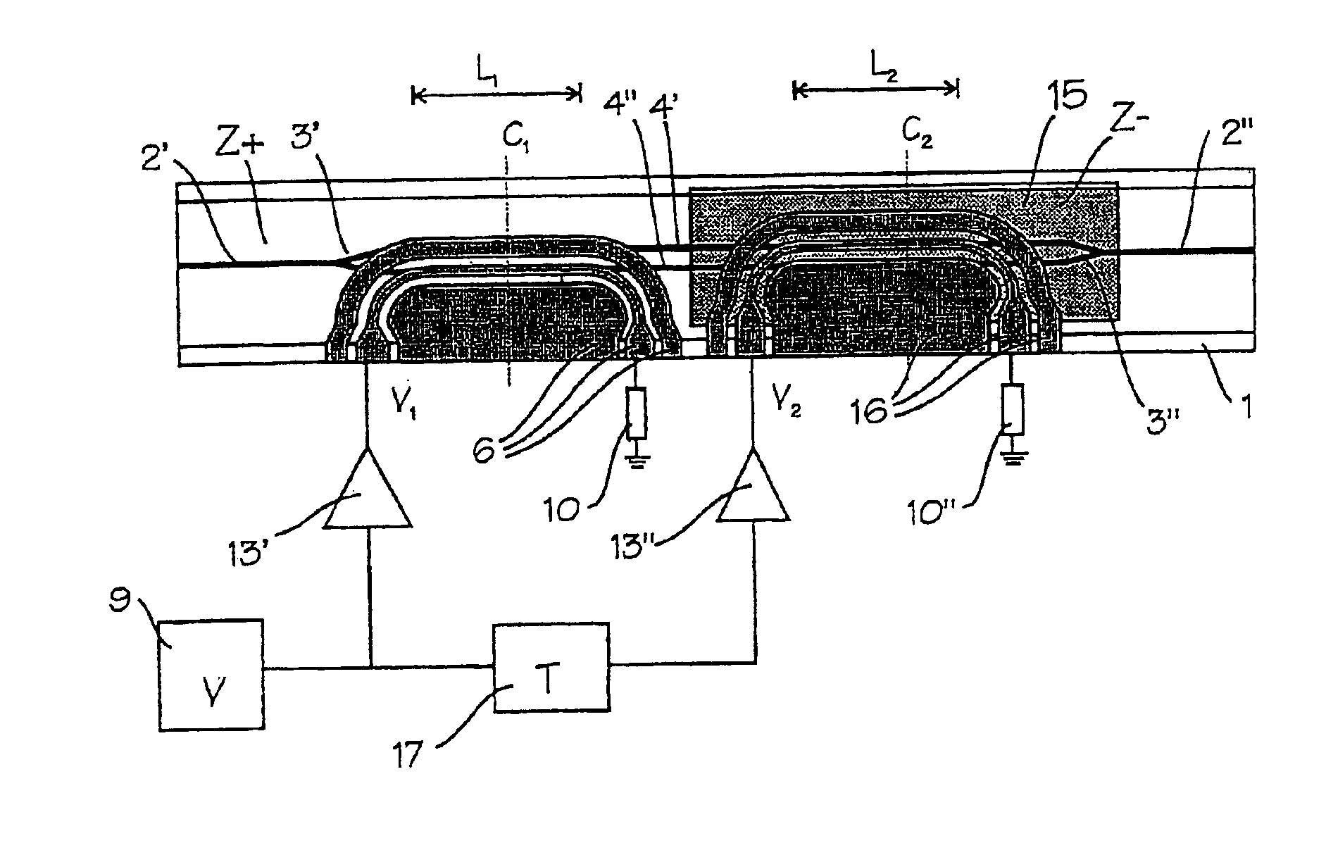
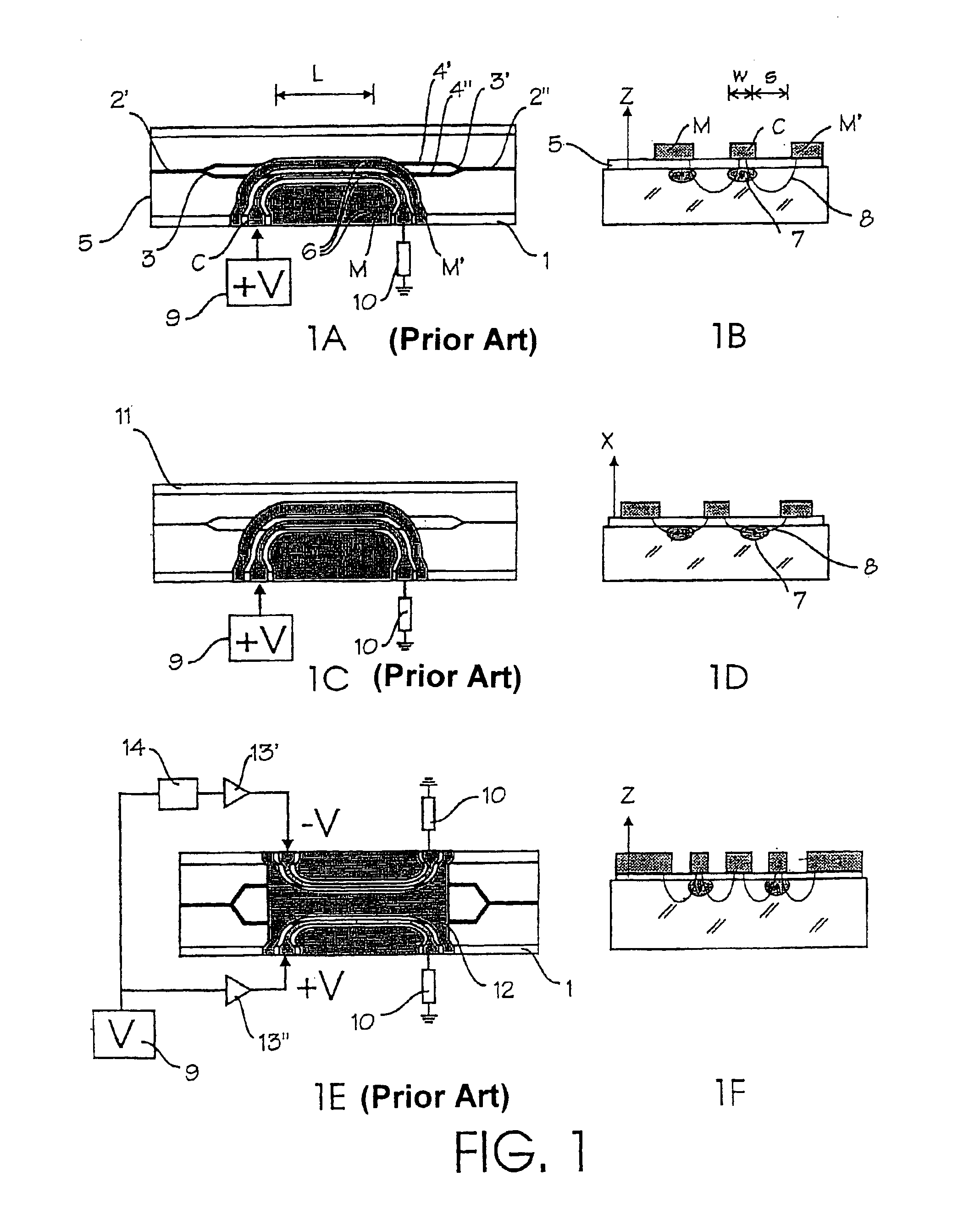
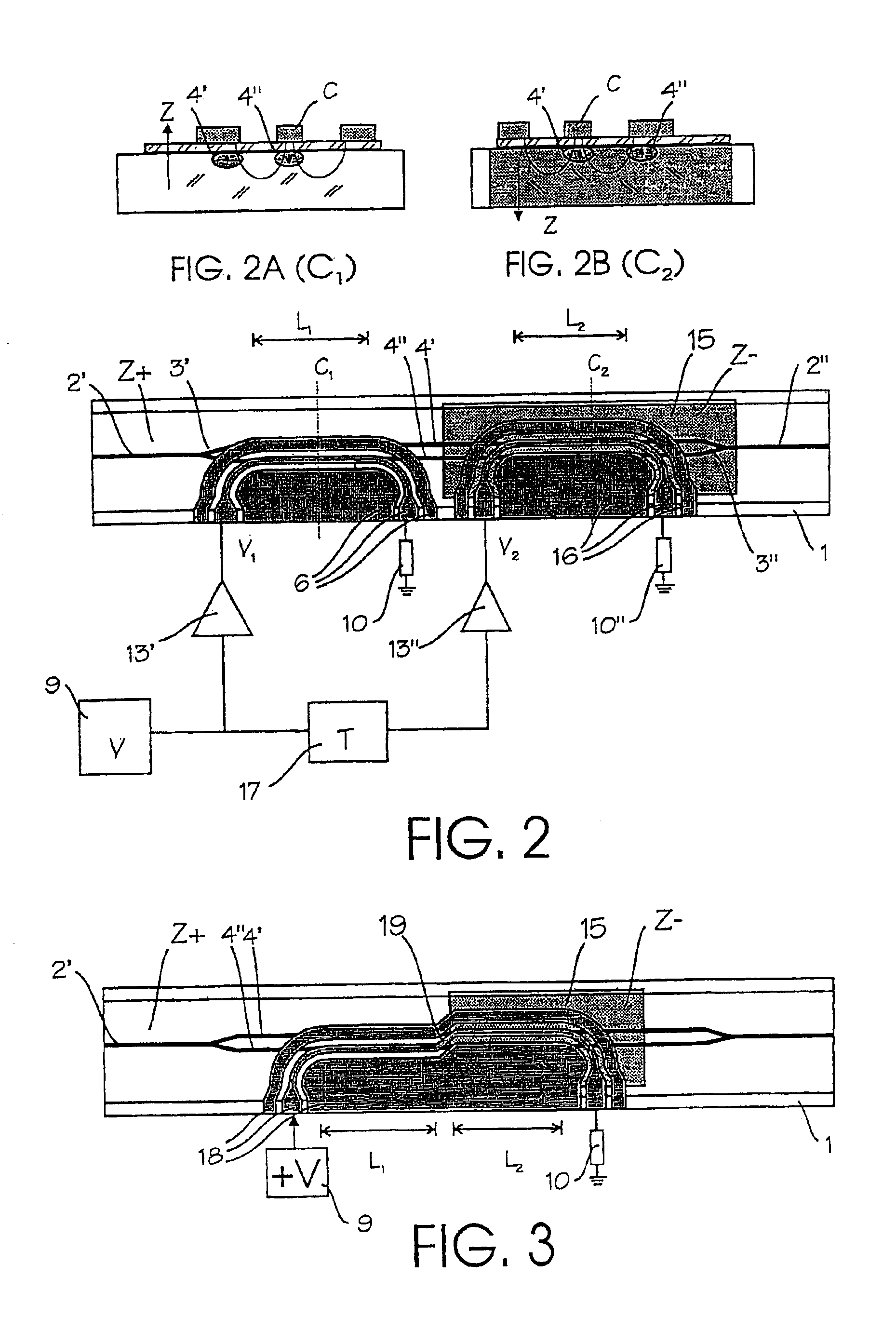
[0060]The component is obtained on a substrate 1 of ferroelectric lithium niobate, of Z section, the axis Z being, for example, oriented positively relative to the main surface of the crystal. It is referred to as orientation Z+. The substrate carries a wave guide pattern of Mach-Zehnder interferometer. This pattern comprises a rectilinear input 2′ and output 2″ guide, two junctions Y, 3′ and 3″, connected by each of the arms 4′ and 4″ of the interferometer. The wave guides are obtained for example by titanium diffusion, or by the method of lithium / protons exchange.

[0061]The lithium niobate crystal comprises in its whole thickness a region 15 which has been subject to an inversion of ferroelectric field. This means that, by short and localised application of an electric field between both faces of the crystal, in the order of 20 kV / mm for a short time period, the spontaneous polarisation of the crystal changes direction permanently. The crystal is thus subject locally to an inversio...


PUM

PropertyMeasurementUnit
widthaaaaaaaaaa
semi-wave voltageaaaaaaaaaa

Abstract

An optical modulator includes a waveguide structure forming a two-wave interferometer made of an electro-optical material, and two arms, a set of electrodes connected to a controllable electric source for applying an electric field on at least one of the arms of the interferometer, so as to vary the phase difference between light waves along one or the other of the two arms. The modulator includes two sets of electrodes placed respectively on each of the interferometer arms, one in the non-reversed region of the electro-optical material, the other in the reversed region, and a delay line placed between the control electronics of the electrode sets introducing a delay equal to the light propagation time in the first electrode set.

Description

BACKGROUND OF THE INVENTION[0001]This invention relates to the field of integrated optoelectronic components applicable particularly in the field of optical telecommunications.[0002]This invention more particularly relates to an electro-optical light modulator liable to be made in particular with lithium niobate. Its configuration requires a cascade structure of two sets of electrodes aligned parallel to a wave guide structure forming a two-arm interferometer for example, a Mach-Zehnder interferometer. A first set is deposited on a portion of crystal whereof the ferroelectric field is oriented with positive (or negative) polarisation, the second set of electrodes being on the other half of the crystal exhibiting a field of negative (or positive) reversed ferroelectric polarisation.DESCRIPTION OF THE RELATED ART[0003]Recent evolutions in optical fibre transmissions require higher and higher channel information flow rates, in the order of 40 Gbit / s. Each channel being in such a case a...

Claims


Application Information

Patent Timeline
Patent Type & Authority Patents(United States)
IPC IPC(8): G02F1/01G02F1/225G02B6/12G02F1/035
CPCG02F1/2255
Inventor PORTE, HENRIHAUDEN, JEROMEMOLLIER, PASCAL
Owner CENT NAT DE LA RECHERCHE SCI
Why Eureka
Try Eureka