Solid-state imaging apparatus and manufacturing method thereof

Inactive Publication Date: 2005-09-27
PANASONIC CORP
View PDF2 Cites 25 Cited by
  • Summary
  • Abstract
  • Description
  • Claims
  • Application Information

AI Technical Summary

Benefits of technology

[0074]When such a structure member is made of a thermoplastic resin and formed by injection molding, deformation is easily produced particularly during a hardening process, and deformation is produced also when a device is used in a high temperature environment, thereby causing a problem in that a connection failure easily occurs in a portion where the solid-state image pickup element is connected to the structure member (thr

Problems solved by technology

Therefore, a conventional apparatus has problems in that many connections must be formed during a process of mounting components and hence the size of the apparatus is made large, and that the mounting process requires a prolonged time period.
However, there is a problem in that fillers, which are often used in order to reduce the coefficient of expansion of a resin material, cannot be added in an amount larger than a given one from the viewpoints of the molding accuracy and the durability of molding dies.
As described above, a conventional solid-state imaging apparatus is configured by externally attaching various function components such as a signal processing circuit, and hence has problems in that the mounting process requires a prolonged time period, and that the size of the device is large.
Moreover, a connection failure occurs in connecting portions between a solid-state image pickup element and components of a processing circuit, and this causes the r

Method used


Image

  • Solid-state imaging apparatus and manufacturing method thereof
  • Solid-state imaging apparatus and manufacturing method thereof
  • Solid-state imaging apparatus and manufacturing method thereof

Examples


embodiment 1

[0090](EMBODIMENT 1)

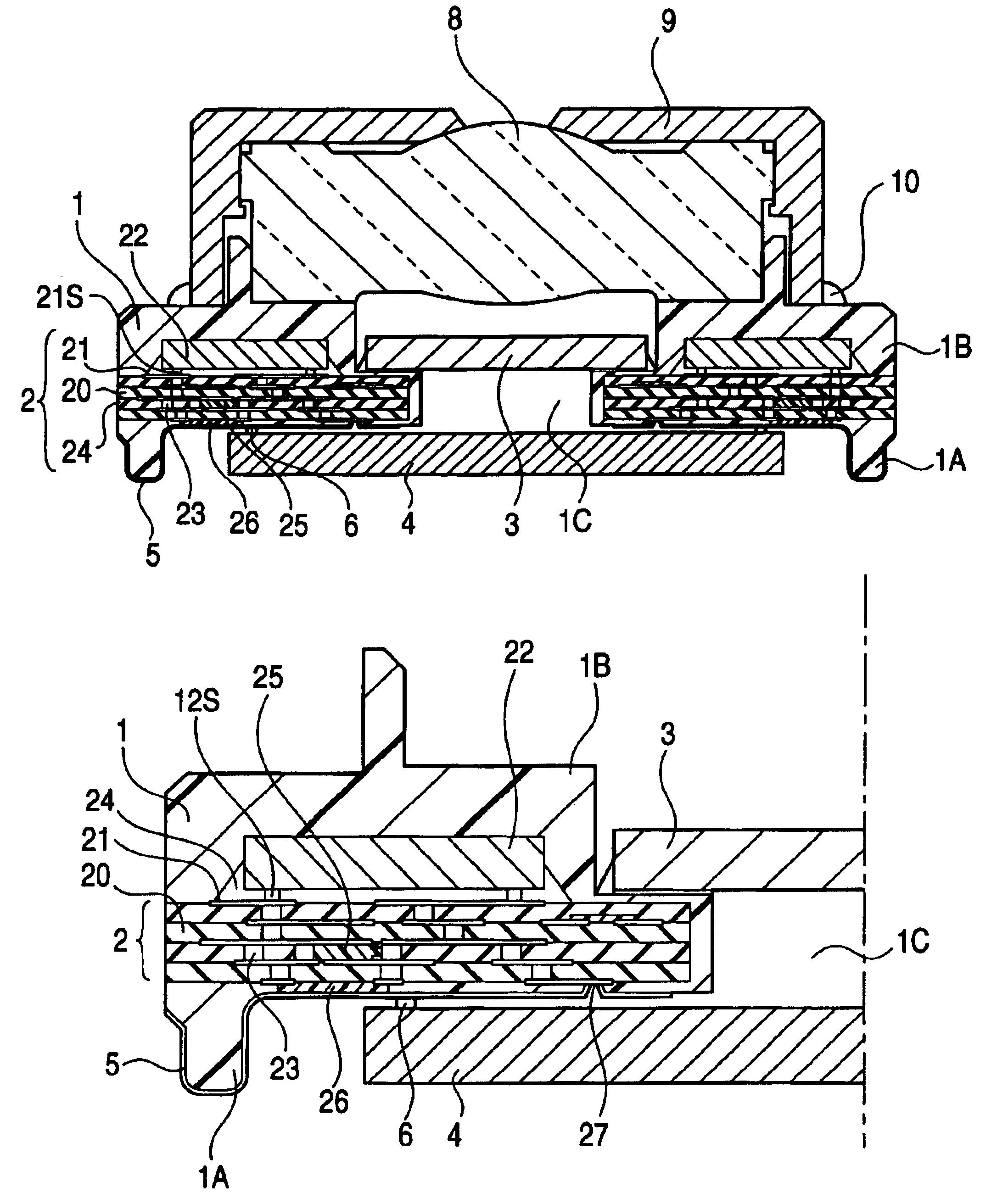
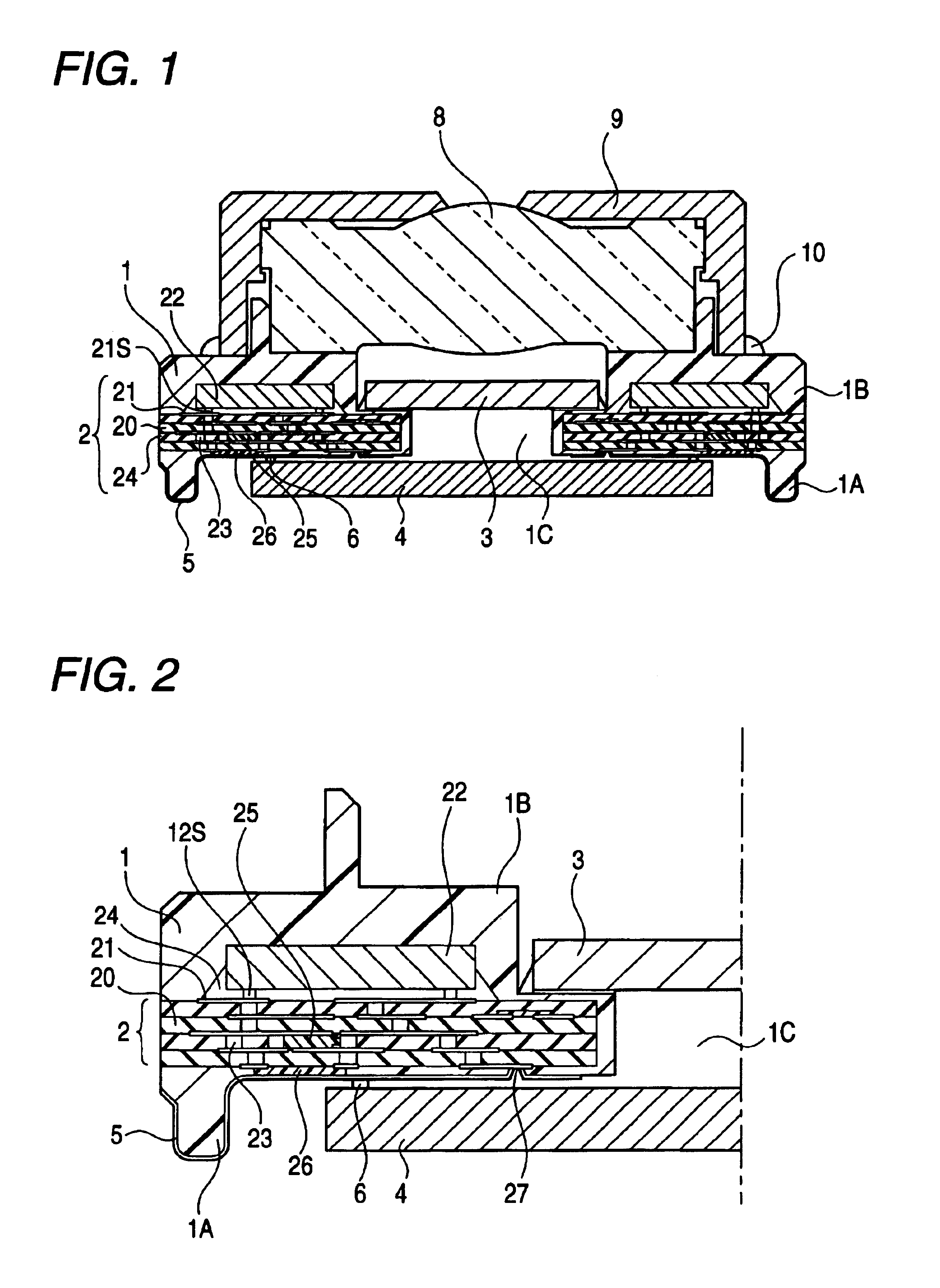
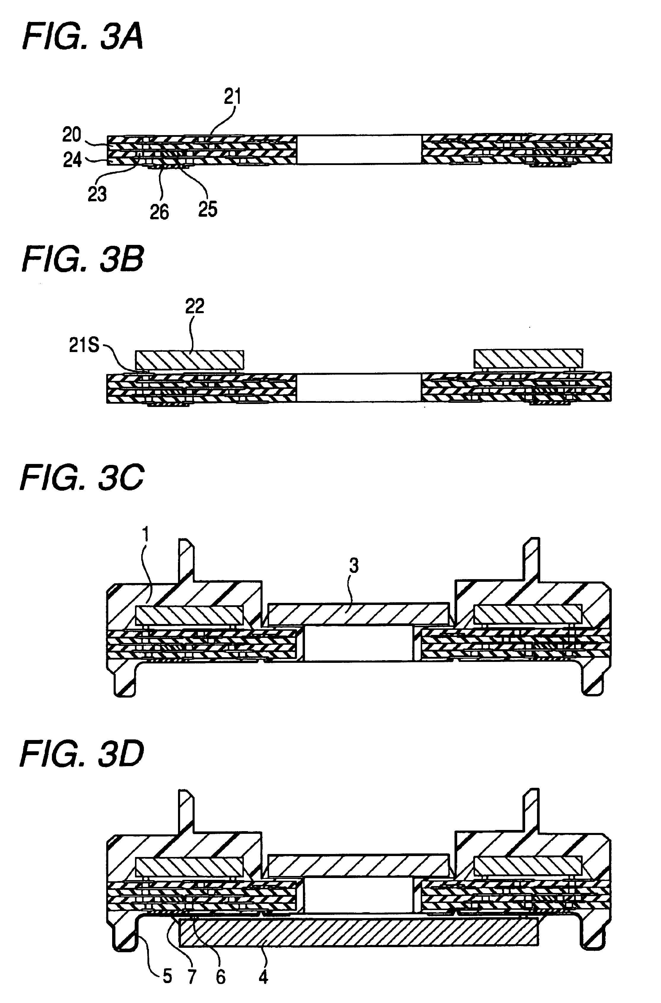
[0091]FIGS. 1 and 2 are views showing main portions of a solid-state imaging apparatus which is a first embodiment of the invention.

[0092]In the solid-state imaging apparatus, in a molding process of a structure member 1 on which a solid-state image pickup element is to be mounted, a multilayer wiring board 2 is sealed together with a signal processing circuit chip DSP 22 formed on a first face of the multilayer wiring board 2, into the structure member 1 configured by an insulating polyphthalamide resin. Incidentally, the multiplayer wiring board serves as a serving circuit board formed a ceramic substrate as a basic member, and the coefficient of thermal expansion of the ceramic substrate is very smaller than that of a resin constituting the structure member. The structure member 1 has a through-opening portion 1C. A plate-like member constituting an optical filter 3 is attached to the structure member 1, includes the signal processing circuit chip DSP 22 there...

embodiment 2

[0113](EMBODIMENT 2)

[0114]FIG. 4 is a view showing main portions of a solid-state imaging apparatus according to a second embodiment of the invention.

[0115]In the first embodiment, the optical filter 3 is attached to the multilayer wiring board. In contrast, according to the second embodiment, the ceramic substrate constituting the multilayer wiring board is made of light-transmitting ceramic, and a desired film is formed on the surface as a multi-refraction material 20S which will be used as an optical filter. The multilayer wiring board which is to be sealed into the structure member is configured in the following manner. The multi-refraction material 20S is used as an insulating substrate, and a multilayer wiring structure member 2M is formed so as to have an annular shape in a peripheral area excluding the area corresponding to the through-opening portion 1C. The multilayer wiring structure member 2M is placed in molding dies, and then injection molding is conducted to seal a ce...

embodiment 3

[0119](EMBODIMENT 3)

[0120]FIGS. 6 and 7 are views showing main portions of a solid-state imaging apparatus according to a third embodiment of the invention. FIG. 7 is a section view taken along the line A—A in FIG. 6.

[0121]In the solid-state imaging apparatus, in a molding process of a structure member 101 on which a solid-state image pickup element 104 is to be mounted, a ceramic substrate 102g and a circuit portion 102 of a multilayer wiring structure formed on a film carrier 120F serving as a flexible substrate are sealed together with a signal processing circuit chip (DSP) 122 formed on a first face of the ceramic substrate 102g via through-holes (not shown) opened in the ceramic substrate 102g, into the structure member 101 configured by an insulating polyphthalamide resin. Incidentally, the ceramic substrate 102g is used as a fixing member, and the coefficient of thermal expansion of the ceramic substrate 102g is very smaller than that of a polyphthalamide resin constituting t...


PUM


Abstract

A structure member is used wherein a circuit board is connected to a solid-state image pickup element and placed between a portion of the structure member to which the solid-state image pickup element is attached, and another portion to which a light-transmitting member is attached, and the circuit board is sealed integrally into the structure member. The solid-state image pickup element is attached to a through-opening portion 1C, and a light-transmitting member is attached so as to cover the through-opening portion 1C with being separated from the solid-state image pickup element by a predetermined distance. In a process of molding the structure member, the circuit board is integrally molded, whereby the manpower can be reduced, and the structures of the attaching portions can be simplified to miniaturize the device.

Description

BACKGROUND OF THE INVENTION[0001]The present invention relates to a solid-state imaging apparatus and a manufacturing method thereof, and more particularly to a small-sized solid-state imaging apparatus including a solid-state image pickup element, such as a surveillance camera, a medical camera, or a vehicle camera, and a manufacturing method thereof.[0002]An imaging apparatus of this kind receives an image through an optical system such as a lens, and outputs the image in the form of an electric signal. Recently, in accordance with miniaturization and enhancement of the performance of such an imaging apparatus, also the size of a camera is reduced, and an imaging apparatus is used in various fields and expands its market as an image inputting device.[0003]In a conventional imaging apparatus using a solid-state image pickup element, each of components such as a lens, the solid-state image pickup element, and an LSI on which a driving circuit for the element and a signal processing ...

Claims


Application Information

Patent Timeline
IPC IPC(8): H01L27/14H01L27/15H01L31/12H01L31/0203H01L33/00H04N5/225H01L27/146
CPCH01L27/14618H01L27/14625H04N5/2257H01L2224/16H01L2924/00014H04N23/57H01L2224/0401H01L27/146H01L27/14
Inventor HARAZONO, FUMIKAZU
Owner PANASONIC CORP
Why Eureka
Try Eureka