
Wiring board comprising granular magnetic film

a granular magnetic film and wire board technology, applied in the field of wire boards, can solve the problems of high-frequency spurious radiation noise, induction and high-frequency noise, and the trend toward lighter weight, thinner profile, and smaller size in electronic components and electronic equipment, and achieve the effect of reducing the noise of high-frequency spurious radiation

Inactive Publication Date: 2005-10-11
TOKIN CORP
View PDF26 Cites 1 Cited by
  • Summary
  • Abstract
  • Description
  • Claims
  • Application Information

AI Technical Summary

Benefits of technology

"The present invention provides flexible wiring boards that have magnetic material effective in countering spurious radiation from semiconductor devices and electronic circuits that operate at high speeds. The magnetic material can be a narrow-band or broad-band magnetic loss material that has a maximum value of loss factor within a specific frequency range and a relative bandwidth not greater than a certain threshold. The magnetic thin film can be made of a composition represented by M—X—Y, where M is at least one of Fe, Co, and Ni, X is at least one element other than M or Y, and Y is at least one of F, N, and O. The magnetic loss material can be effective in reducing interference and improving the performance of high-speed electronic devices."

Problems solved by technology

In these active devices, higher speeds are being achieved at a prodigious rate in terms of calculating speed and signal processing speed, and the electrical signals propagated through the high-speed electronic circuits have become a major cause of inductive and high-frequency noise because of the rapid voltage and current changes associated therewith.
Meanwhile, the trend toward lighter weight, thinner profile, and smaller size in electronic components and electronic equipment continues rapidly and unabatedly.
Accordingly, electronic devices and signal lines that are integrated or mounted overly densely become extremely close to each other, and the situation is now such that, in conjunction with the higher signal processing speeds being achieved, as remarked earlier, high-frequency spurious radiation noise is easily induced.
Problems have been pointed out with spurious radiation from power supply lines going to active devices in such recent electronic integrated devices and wiring boards, against which such measures as the insertion of decoupling condensers or other concentrated constant components into the power lines have been implemented.
However, because the noise generated in higher speed implementations of electronic integrated devices and wiring boards contains harmonic components, signal paths exhibit a distributed constant behavior, and situations have arisen where measures against noise that presume conventional concentrated constant circuits are ineffective.
Similar problems have arisen also, inside electronic equipment, relating to connections between boards, and to the flexible wiring or printed circuit boards (FPCs) or flexible flat cables (FFCs) (hereinafter both referred to by the generic term flexible wiring or printed circuit board (FPC)) mounted to electronic components.

Method used


Image

  • Wiring board comprising granular magnetic film
  • Wiring board comprising granular magnetic film
  • Wiring board comprising granular magnetic film

Examples


second embodiment

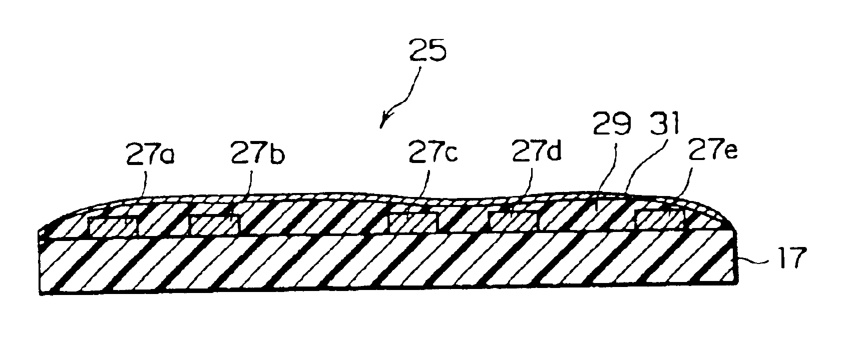
[0050]Referring to FIG. 3, a flexible wiring board 25 according to the present invention is like a conventional flexible wiring board in that conductor patterns 27a, 27b, 27c, 27d, and 27e of copper or other conductive metal are deployed on the flexible base material 17 of a polyimide or the like.

[0051]However, in the flexible wiring board 25 according to the second embodiment of the present invention, an insulation layer 25 is deployed which consists of a synthetic resin or the like so as to cover the entire surface on the side where the conductor patterns 27a, 27b, 27c, 27d, and 27e are deployed, inclusive of the conductor patterns 27a, 27b, 27c, 27d, and 27e, and on the surface of that insulation layer 25 is formed a granular magnetic thin film 31, by vapor deposition or the like, across the entirety thereof. If necessary, moreover, such can be formed in one part only.

[0052]In the flexible wiring boards 15 and 25 according to the first and second embodiments having such configura...

third embodiment

[0070]Referring to FIG. 6, a multi-layer printed wiring or interconnection board 51, which will be hereinafter referred to as multiplayer printed wiring board, according to the present invention has a laminar structure wherein a first to a fifth printed wiring board 53, 55, 57, 59, and 61 are stacked up. A granular magnetic thin film 65 is formed across the entire surface of a ground pattern 63 deployed on one surface of the first printed wiring board 55 that consists of a glass epoxy material. A conductor pattern 67, on the other hand, is formed on the surface that is on the opposite side from the ground pattern 63 on the printed wiring board. On that conductor pattern 67, further, are formed granular magnetic thin films 65. And on those surfaces is formed a second printed wiring board 53 made of a glass epoxy material. This second printed wiring board 53 is essentially an insulating board that has no conductor pattern. The second printed wiring board 53 does not have the conductor...

fourth embodiment

[0077]Making reference to FIG. 7, a multi-layer wiring board 69 according to the present invention has first to fifth printed wiring boards 55, 53, 57, 59, and 61, having a polyimide as their base material, formed in laminar fashion. The second printed wiring board 53 deployed below the first printed wiring board 55 comprises a ground pattern 63 on one surface thereof, and a conductor pattern 67 on the other surface thereof. On the ground pattern of the second printed wiring board 53 is formed a granular magnetic thin film 65 across the entire surface thereof. On the conductor pattern on the other surface of the second printed wiring board 53, meanwhile, granular magnetic thin films 65 are formed, and thereupon is stacked one surface side of the first printed wiring board 55. On the other surface side of the first printed wiring board 55 are formed the third and fourth printed wiring boards 57 and 59, each having conductor patterns 67 on one side thereof. On those conductor patterns...


PUM


Abstract

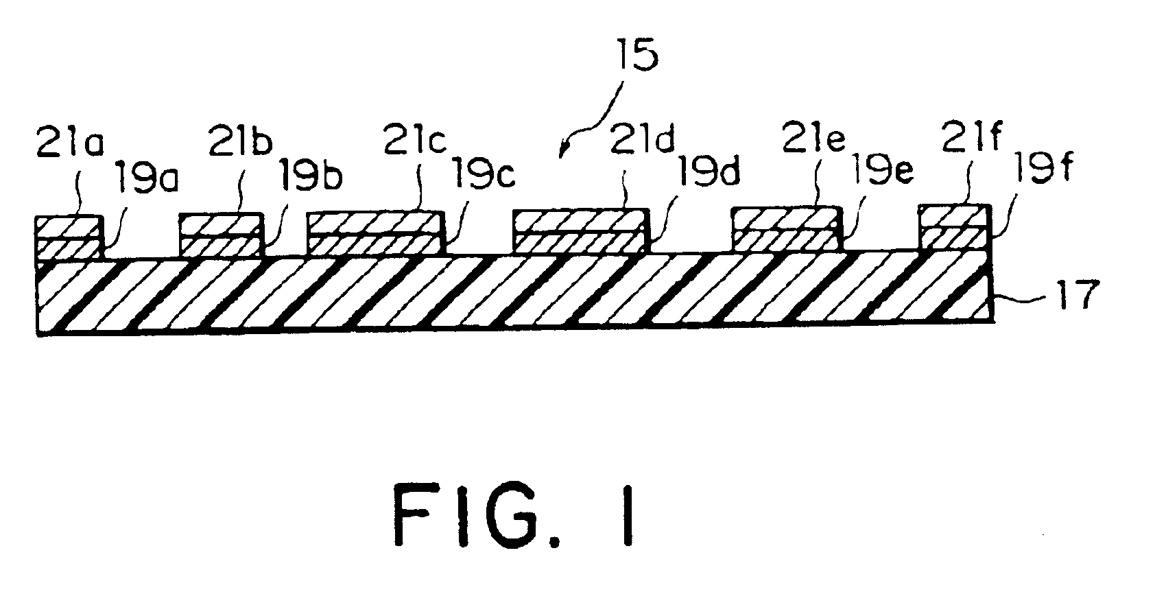
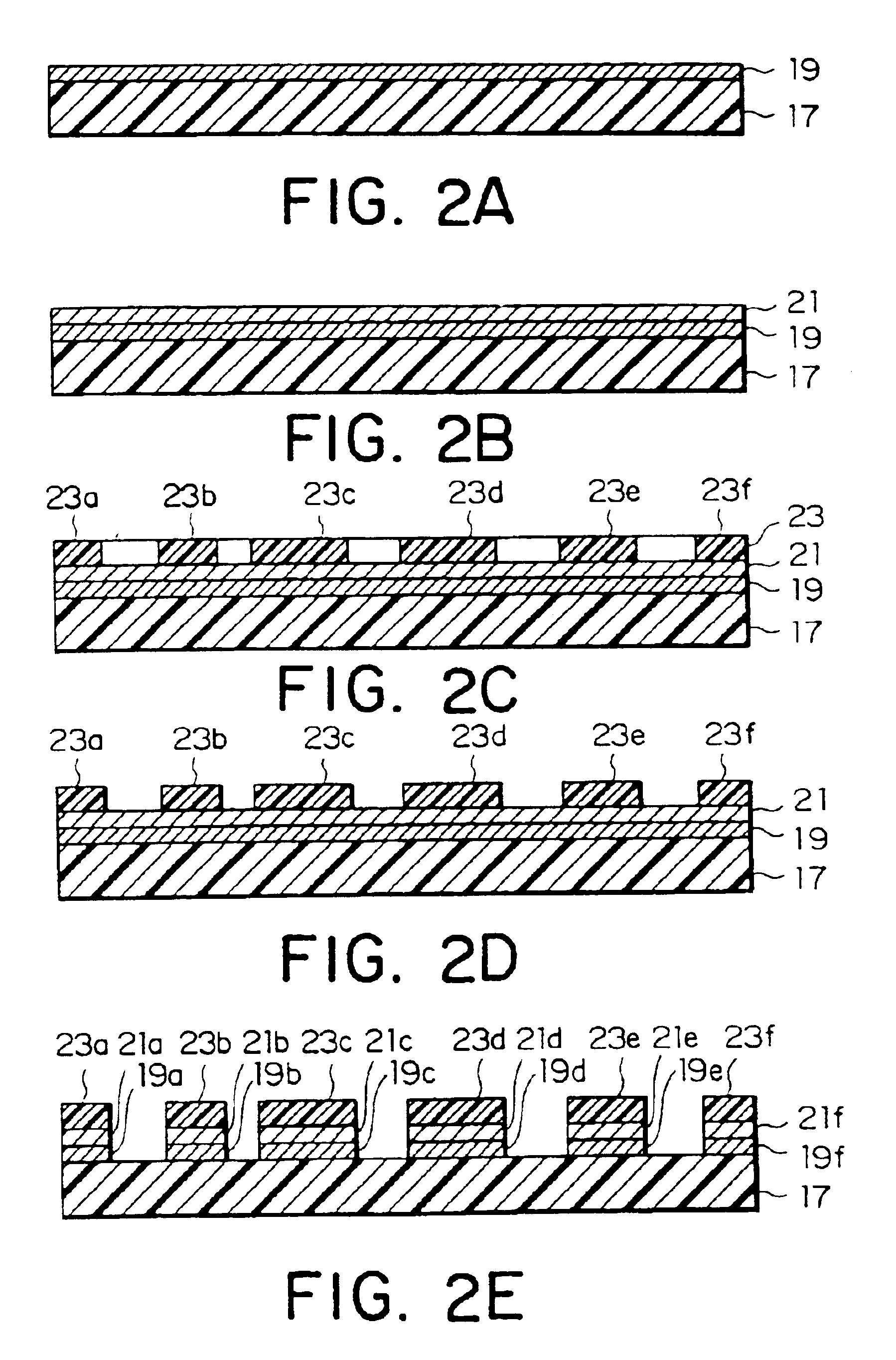
In order to provide a wiring board comprising a magnetic material effective in suppressing spurious radiation in semiconductor devices and electronic circuits and the like that operate at high speeds, a wiring board (15) comprises an insulative base material (17), conductor patterns (19a to 19f) formed thereon, and magnetic thin films (21a to 21f) formed on the conductor patterns (19a to 19f. The magnetic thin film is configured of a magnetic loss material represented by M—X—Y, where M is at least one of Fe, Co, and Ni, X is at least one element other than M or Y, and Y is at least one of F, N, and O, the maximum value μ″max of the loss factor μ″ that is an imaginary component in the complex permeability characteristic of the magnetic loss material exists within a frequency range of 100 MHz to 10 GHz, and a relative bandwidth bwr is not greater than 200% or not smaller than 150% where the relative bandwidth bwr is obtained by extracting a frequency bandwidth between two frequencies at which the value of μ″ is 50% of the maximum μ″max and normalizing the frequency bandwidth at the center frequency thereof.

Description

[0001]This application is a divisional of application Ser. No. 09 / 825,418, filed 3 Apr. 2001 now U.S. Pat. No. 6,653,573, a Convention application based on Japanese applications 101756 and 101765, both filed 4 Apr. 2000.BACKGROUND OF THE INVENTION[0002]1. Field of the Invention[0003]This invention relates to wiring boards that comprise magnetic bodies that exhibit outstanding magnetic loss characteristics at high frequencies, and more particularly to wiring boards such as flexible wiring boards and flexible flat cables that comprise multilayer or unilayer wiring boards or high-frequency current suppression bodies wherein magnetic loss materials are used that exhibit outstanding complex permeability characteristics and are effective in suppressing electromagnetic interference and spurious radiation that are problematic in active devices that operate at high speed, high-frequency electronic components, and electronic equipment mounted thereon.[0004]2. Description of the Related Art[00...

Claims


Application Information

Patent Timeline
Patent Type & Authority Patents(United States)
IPC IPC(8): H05K3/24H05K1/02
CPCH05K1/0233H05K3/244H05K1/02
Inventor AWAKURA, YOSHIOWATANABE, SHINYASHIRATORI, SATOSHIONO, HIROSHI
Owner TOKIN CORP
Learn More