Optical switch including two integrated multiphase SLM's and a wave-plate the wave-plate providing an optical retardance of (2n+1)lambda/4

a multi-phase, optical retardance technology, applied in the field of optical switching, can solve the problems of limited switching for achieving the required switching, relatively poor noise performance, and only 40.5% of the theoretical diffraction efficiency of a binary phase devi

Inactive Publication Date: 2005-10-11
THOMAS SWAN & CO LTD
View PDF9 Cites 30 Cited by
  • Summary
  • Abstract
  • Description
  • Claims
  • Application Information

AI Technical Summary

Problems solved by technology

Many switches for achieving the required switching are limited in functional size to less than 64×64, and / or suffer from relatively poor noise performance.
There are however a number of practical design problems associated with the migration from a static optical shuffle to a reconfigurable switch.
However, the maximum theoretical diffraction efficiency for a binary phase device is only 40.5%.
This type of SLM typically operates in reflection rather than transmission, and the switch layout shown in FIG. 1 is therefore no longer appropriate.

Method used


Image

  • Optical switch including two integrated multiphase SLM's and a wave-plate the wave-plate providing an optical retardance of (2n+1)lambda/4
  • Optical switch including two integrated multiphase SLM's and a wave-plate the wave-plate providing an optical retardance of (2n+1)lambda/4
  • Optical switch including two integrated multiphase SLM's and a wave-plate the wave-plate providing an optical retardance of (2n+1)lambda/4

Examples


first embodiment

[0079]Referring now to FIG. 4, an integrated spatial light modulator in accordance with the invention will now be described:

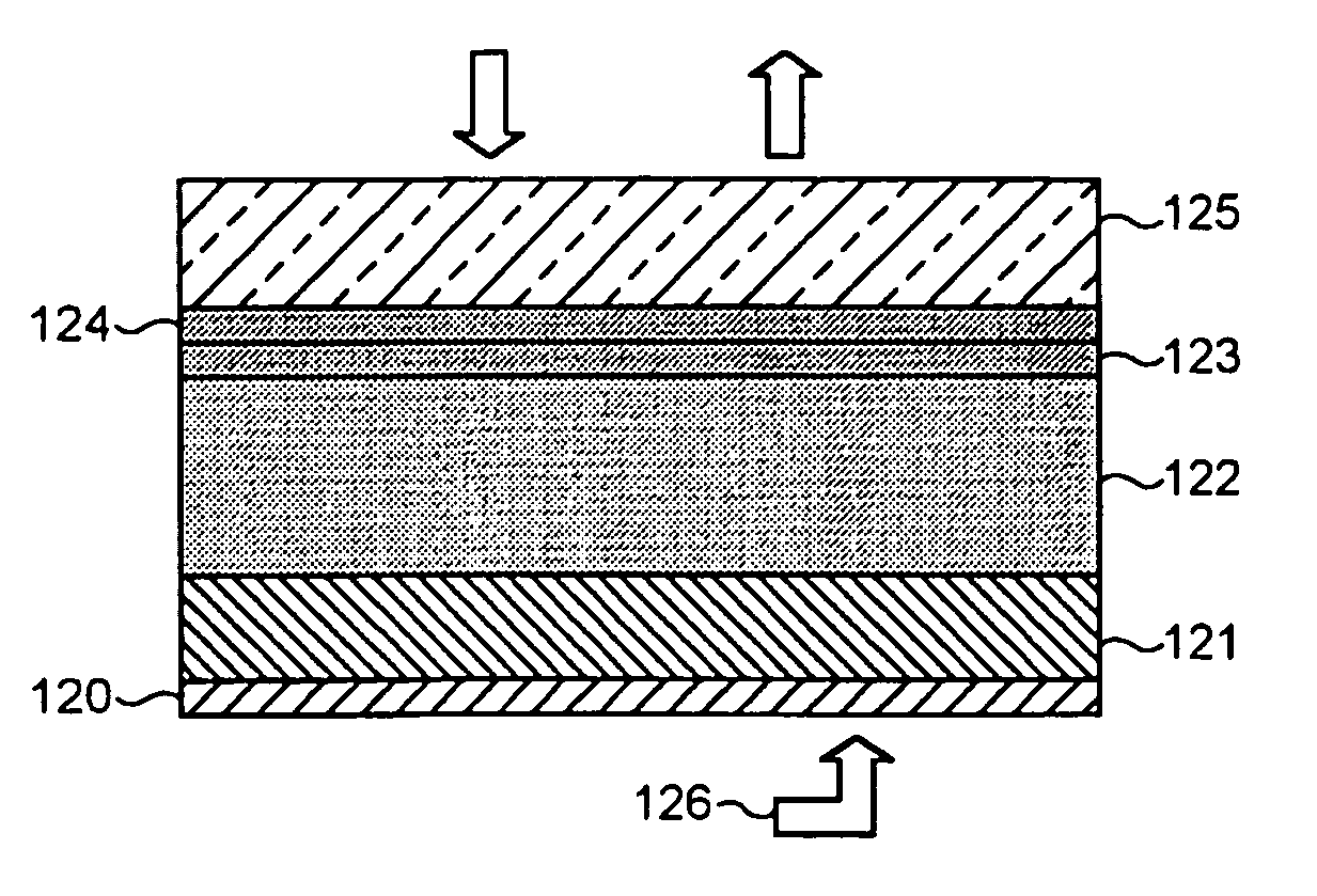
[0080]AS seen in FIG. 4, the SLM consists of an aluminium pad 120, which forms a pixel array, and is connected to pixel driving circuitry by a connection figuratively shown at 126. On the pixel array 120 there is disposed a quarter-wave plate 121. On the quarter-wave plate, and over an intervening alignment layer, (not shown) there is disposed a liquid crystal layer 122—here a nematic liquid crystal is used, but the invention is not so limited. The actual requirement is the ability to provide an out of plane tilt. On the liquid crystal layer there is disposed an alignment layer 123, as known to those skilled in the art, and over the alignment layer there is disposed a transparent conductive layer 124 such as an ITO (Indium Tin Oxide) layer forming a common electrode plane, and an upper glass layer 125.

[0081]The quarter-wave plate can be deposited on the pixel a...

second embodiment

[0082]A second embodiment is shown in FIG. 5.

[0083]Referring to FIG. 5, a pixel array 130 is integrated on a silicon-1.5 μm-transparent backplane structure 131, and is sandwiched between the backplane structure and one face of a liquid crystal layer 132. The other side of the liquid crystal layer 132 is in contact with an alignment layer 133, which in turn is covered by an ITO layer 134. A quarter wave-plate 135 is disposed between a front aluminium mirror 136 and the ITO electrode 134. The thickness of the quarter wave plate may be adjusted by spin-coating techniques so that in reflection it functions as a half-wave plate at λ=1.57 μm.

[0084]An embodiment of a spatial light modulator in accordance with FIG. 5 was constructed. The pixels were constructed using the polysilicon layer of a conventional 2 μm CMOS process. FIG. 6 shows an overview of the silicon backplane layout.

[0085]Referring to FIG. 7 a further embodiment of the invention uses a twisted nematic liquid crystal mixture i...

third embodiment

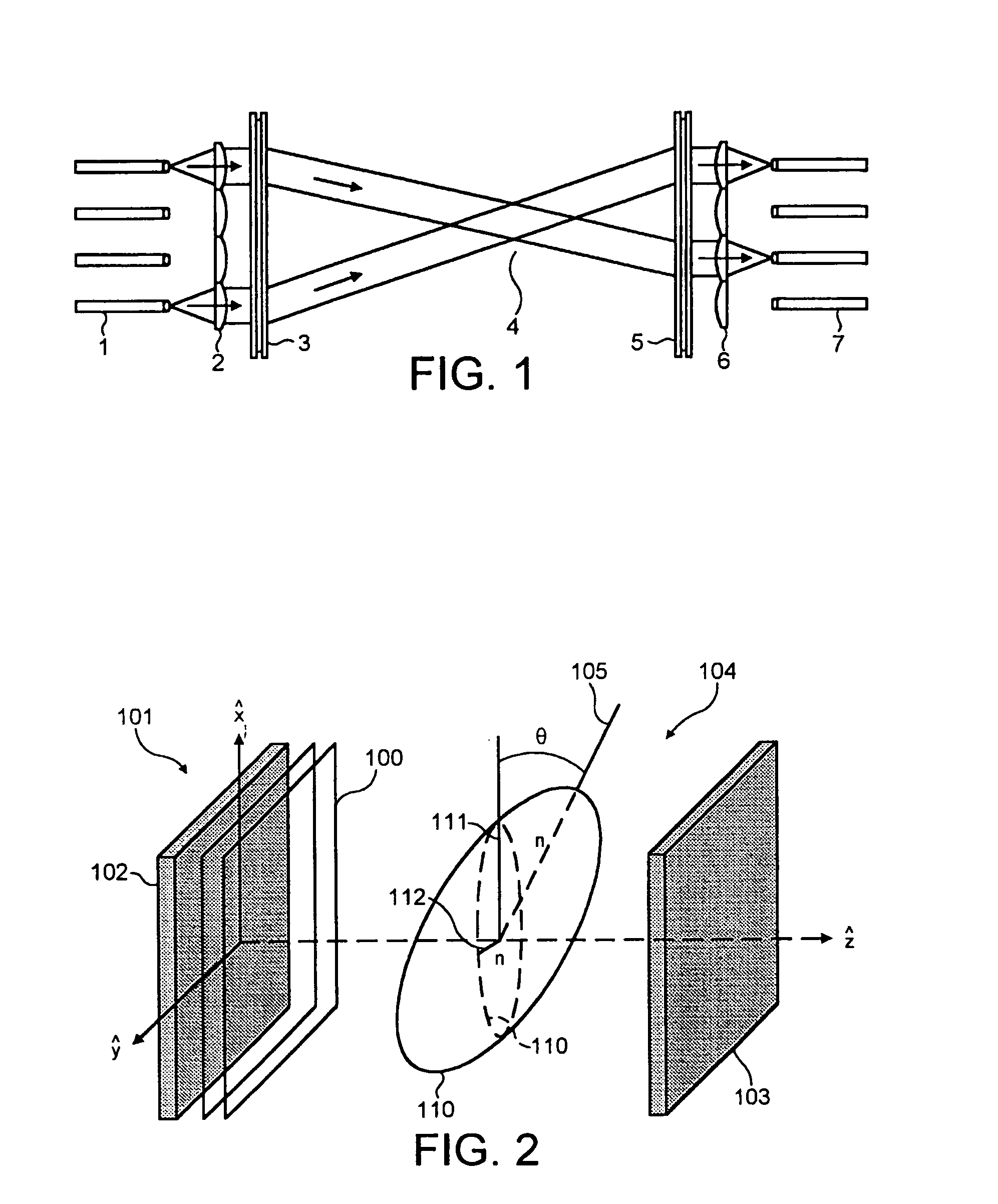
[0107]Referring to FIG. 13, an optical switch according to the invention has the second SLM 141 offset by half a hologram's width in one plane (e.g. the x direction). Thus zero-order crosstalk 145, including the polarisation-dependent zero order, is directed at a point midway 149 between output fibres. In this case the zero-order crosstalk is subject to an offset of s / 2, with a corresponding additional attenuation dependent on the offset.

[0108]The third embodiment is most appropriate in the presence of good surface flatness on the SLM. For the case of offset loss, it reduces as the ratio of the spot-size to the fibre separation is increased. In any final design there will be an optimum value of this ratio to obtain the overall required system performance.

[0109]Referring now to FIG. 14, in a further embodiment a further reduction of the zero order is achieved by offsetting the output SLM 141 with respect to the input SLM 140 by a whole SLM's height (or more) in the direction normal t...


PUM

PropertyMeasurementUnit
optical retardanceaaaaaaaaaa
voltageaaaaaaaaaa
deflection angleaaaaaaaaaa

Abstract

An optical switch uses a polarization insensitive spatial light modulator operating by a double pass through a liquid crystal cell. The switch includes two such modulators in a cross bar arrangement. Different embodiments employing techniques for reducing cross talk are described.

Description

CROSS REFERENCE[0001]This application is a PCT National Phase Application the claims priority from PCT / GB00 / 03796 having an International filing date of 4 Oct. 2000 which in turn claims priority from UK patent application 9923428.8 filed 4 Oct. 1999.FIELD OF THE INVENTION[0002]The invention relates to the general field of optical switching and more particularly to optical switching using multiphase or continuous phase hologram devices.BACKGROUND OF THE INVENTION[0003]Optical fibre switching components are fundamental to modern global information systems. Single-stage matrix switches operating independently of the optical bit-rate and modulation formats, capable of reconfigurably interconnecting N optical inputs to M optical outputs (where N and M are generally, but not necessarily the same number), are particularly attractive. Many switches for achieving the required switching are limited in functional size to less than 64×64, and / or suffer from relatively poor noise performance. On...

Claims


Application Information

Patent Timeline
Patent Type & Authority Patents(United States)
IPC IPC(8): G02F1/31G02B6/32G02B6/35G02B6/26G02F1/29G02B5/32G03H1/08G02F1/13G02F1/139G02F1/141G02F1/13363
CPCG02B5/32G02B6/264G02B6/32G02F1/31G03H1/02G03H1/08G03H1/2294G02F1/136277G02F1/1393G02F1/1395G02F1/141G02F2001/133638G02F2203/02G02F2203/12G02F2203/50G03H1/0005G03H2001/0224G03H2001/0825G03H2001/085G03H2001/221G03H2001/261G03H2001/306G03H2222/31G03H2222/32G03H2222/34G03H2223/19G03H2223/20G03H2225/22G03H2225/32G03H2225/52G03H2227/03H04Q2213/1301H04Q2213/1319G03H2210/20G03H2240/41G02F1/133638
Inventor CROSSLAND, WILLIAMHOLMES, MELANIEMANOLIS, ILIASWILKINSON, TIMOTHYREDMOND, MAURAROBERTSON, BRIAN
Owner THOMAS SWAN & CO LTD
Why Eureka
Try Eureka