Method and apparatus for forming an electrical contact with a semiconductor substrate

a technology of semiconductor substrate and electrical contact, applied in the field of methods, can solve the problems of contaminating particles, high voltage drop and failure, and conventional plating systems such as described above, and achieve the effect of reliable and reliable manner

Inactive Publication Date: 2005-10-25
NOVELLUS SYSTEMS
View PDF15 Cites 37 Cited by
  • Summary
  • Abstract
  • Description
  • Claims
  • Application Information

AI Technical Summary

Benefits of technology

[0014]It is a further object of the present invention to provide a method and apparatus that plates a semiconductor workpiece such as wafers, flat panels, and magnetic films...

Problems solved by technology

However, conventional plating systems such as described above have many drawbacks and disadvantages.
For example, during the plating process, metal from the plating solution may be electroplated on the contact fingers, thereby generating contaminating particles.
In addition, the electroplated metal on the contact fingers increases contact ...

Method used


Image

  • Method and apparatus for forming an electrical contact with a semiconductor substrate
  • Method and apparatus for forming an electrical contact with a semiconductor substrate
  • Method and apparatus for forming an electrical contact with a semiconductor substrate

Examples


Embodiment Construction

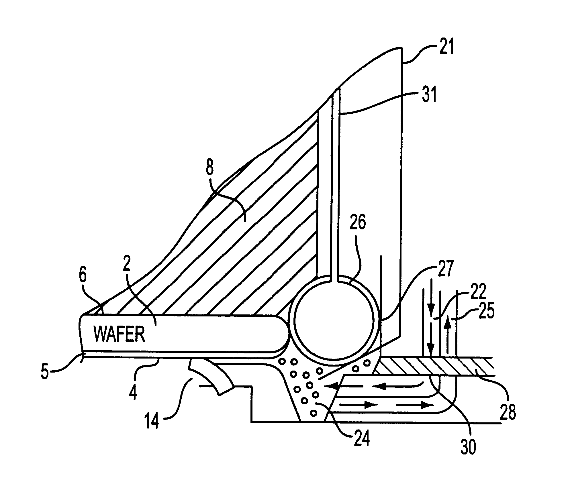
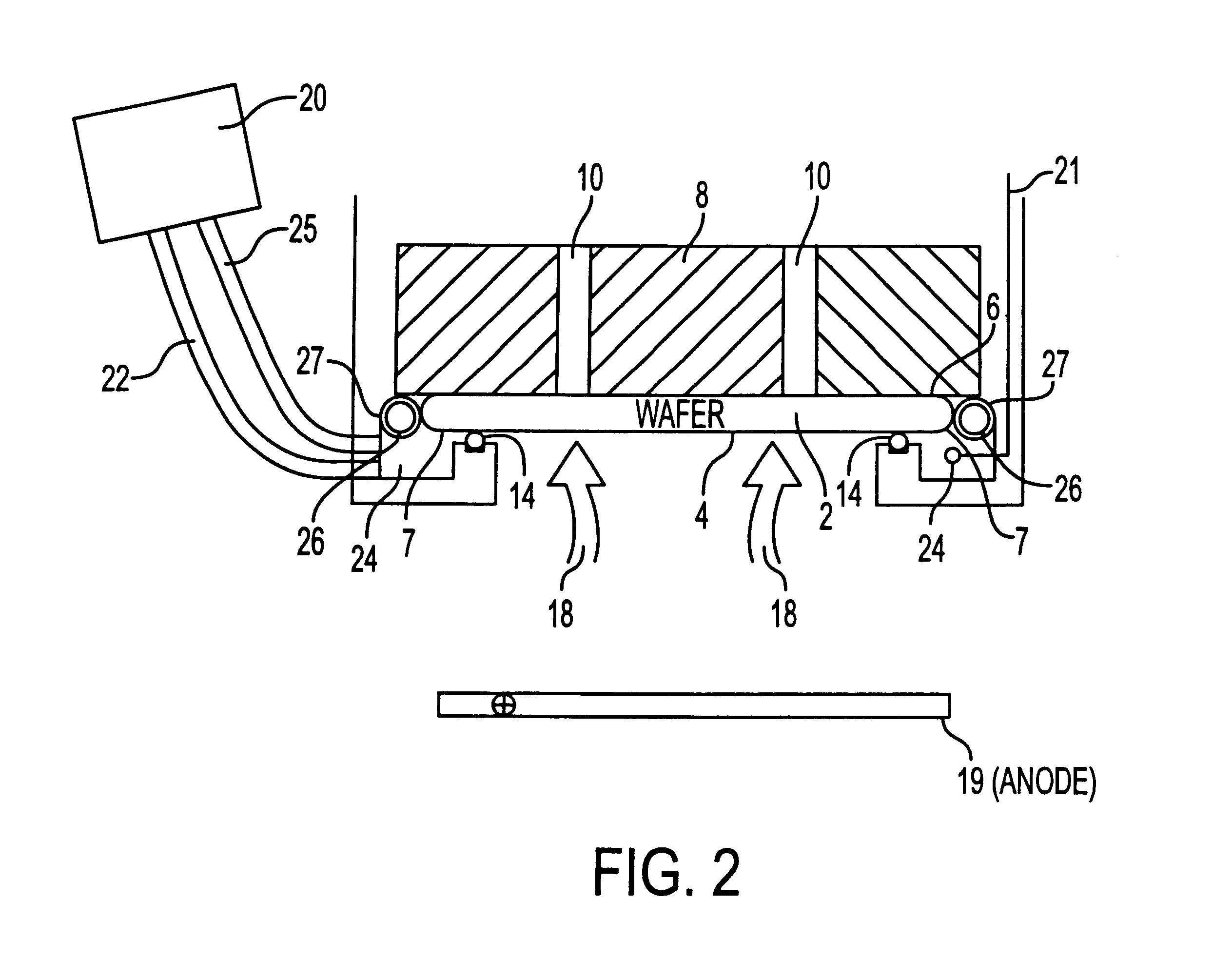
[0028]The preferred embodiments of the present invention will now be described with reference to FIGS. 2-7, wherein like components are designated by like reference numerals throughout the various figures. In the first embodiment, the present invention is directed to a method and apparatus that uses a liquid conductor as electrical contacts on the wafer during the wafer plating process. The liquid conductor is preferably a solution containing indium, tin, gallium, mercury, acid, salt solution, or the like. Other alloys containing indium, tin, gallium, mercury, acid, salt solution, or the like may be used in accordance with the present invention. Since the liquid conductor should be in liquid phase at operating temperature and during the plating process, the melting point thereof will typically be in the range of 10° C. to 40° C.

[0029]In addition to the various types of solutions mentioned above, metal powders mixed with another solution may be used in accordance with the present inv...


PUM

PropertyMeasurementUnit
Lengthaaaaaaaaaa
Electrical conductivityaaaaaaaaaa
Areaaaaaaaaaaa

Abstract

The present invention is directed to a method and apparatus for plating a surface of a semiconductor workpiece (wafer, flat panel, magnetic films, etc.) using a liquid conductor that makes contact with the outer surface of the workpiece. The liquid conductor is stored in a reservoir and pump through an inlet channel to the liquid chamber. The liquid conductor is injected into a liquid chamber such that the liquid conductor makes contact with the outer surface of the workpiece. An inflatable tube is also provided to prevent the liquid conductor from reaching the back face of the workpiece. A plating solution can be applied to the front face of the workpiece where a retaining ring/seal further prevents the plating solution and the liquid conductor from making contact with each other. In an alternative embodiment, electrical contacts may be formed using an inflatable tube that has either been coated with a conductive material or contains a conductive object. The inflatable tube further provides uniform contact and pressure along the periphery of the workpiece, which may not necessarily be perfectly flat, because the tube can conform according to the shape of the periphery of the workpiece. Further, the present invention can be used to dissolve/etch a metal layer from the periphery of the workpiece.

Description

[0001]This is a continuation of application Ser. No. 09 / 877 335 filed Jun. 7, 2001, now U.S. Pat. No. 6,471,847, which is a division of application Ser. No. 09 / 283,024 filed Mar. 30, 1999, now U.S. Pat. No. 6,251,235.FIELD OF THE INVENTION[0002]The present invention relates generally to a method and apparatus for electroplating a metal on a semiconductor substrate. More particularly, the present invention is directed to a method and apparatus for forming electrical contacts on the semiconductor substrate using a liquid conductor during the plating process. Alternatively, electrical contacts may be formed using an inflatable tube that has either been coated with a conductive material or contains a conductive object. Furthermore, the present invention provides a method and apparatus for dissolving / etching a metal layer from the substrate edge.BACKGROUND OF THE INVENTION[0003]Plating is an important and necessary step in the high performance chip fabrication process. When plating, it i...

Claims


Application Information

Patent Timeline
IPC IPC(8): H01L21/00
CPCH01L21/2885H01L21/67075H01L21/6715C25D17/001
Inventor TALIEH, HOMAYOUNBASOL, BULENT
Owner NOVELLUS SYSTEMS
Why Eureka
Try Eureka