Flash memory cell and method of manufacturing the same, and programming/erasing/reading method in the flash memory cell

Inactive Publication Date: 2005-11-01
SK HYNIX INC
View PDF27 Cites 4 Cited by
  • Summary
  • Abstract
  • Description
  • Claims
  • Application Information

AI Technical Summary

Benefits of technology

[0012]The present invention is contrived to solve the above problems and an object of the present invention is to provide a flash memory cell and method of manufacturing the same, and programming/erasing/reading method in the flash memory cell, by which damage of a tunnel oxide film due to an ion implantation process can be prevented by first forming a source region and a drain region a

Problems solved by technology

The flash memory cell constructed above is formed by exposure/etching process several times. Therefore, there are problems that the process steps are complicated and obtaining a process margin is difficult.
In addition, the conventional flash memory cell requires a large area compared to peripheral devices and only data of one bit per cell can be stored.
Due to this, there is a problem that the efficiency is degraded in view of the level of inte

Method used


Image

  • Flash memory cell and method of manufacturing the same, and programming/erasing/reading method in the flash memory cell
  • Flash memory cell and method of manufacturing the same, and programming/erasing/reading method in the flash memory cell
  • Flash memory cell and method of manufacturing the same, and programming/erasing/reading method in the flash memory cell

Examples


Embodiment Construction

[0039]The present invention will be described in detail by way of a preferred embodiment with reference to accompanying drawings, in which like reference numerals are used to identify the same or similar parts.

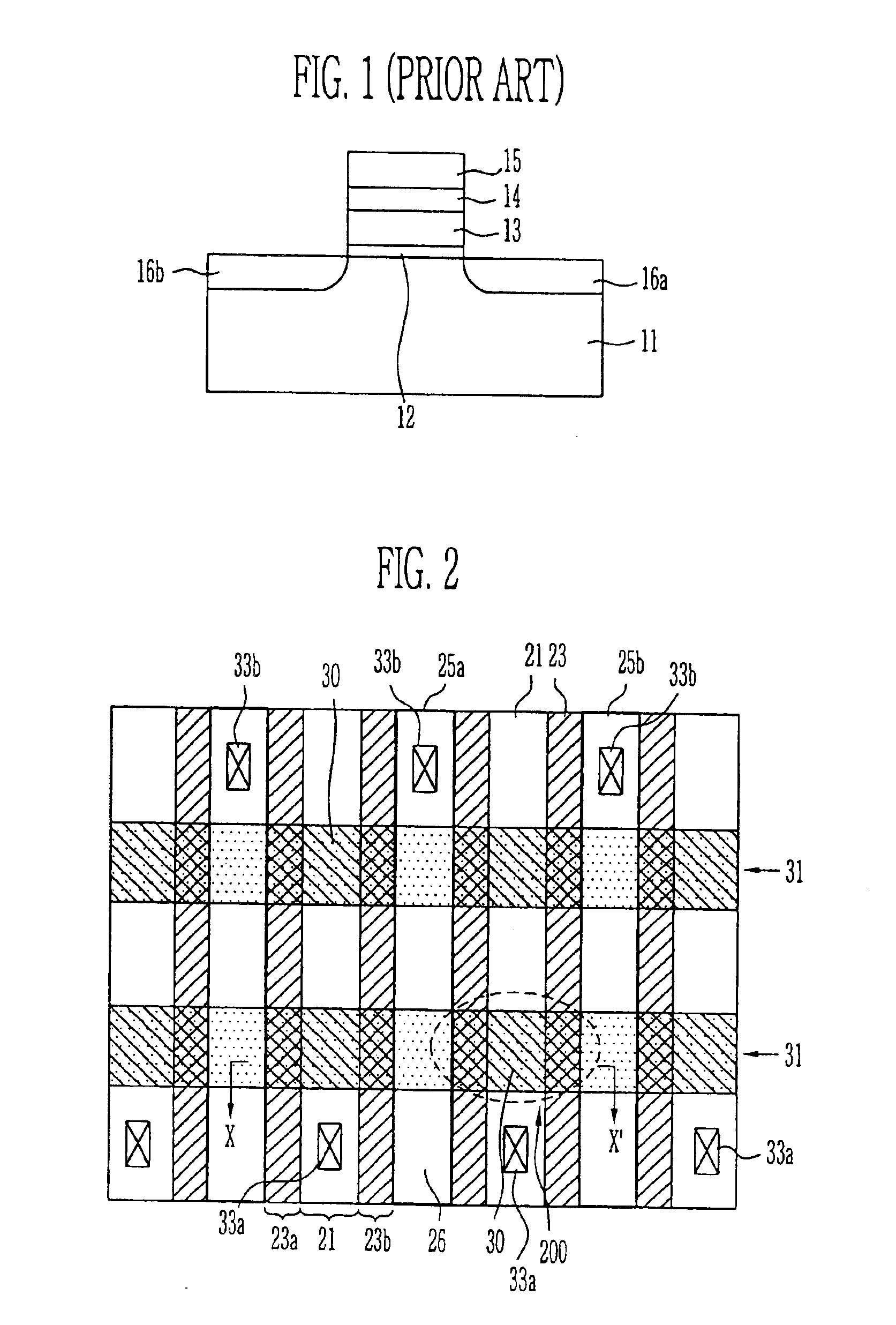
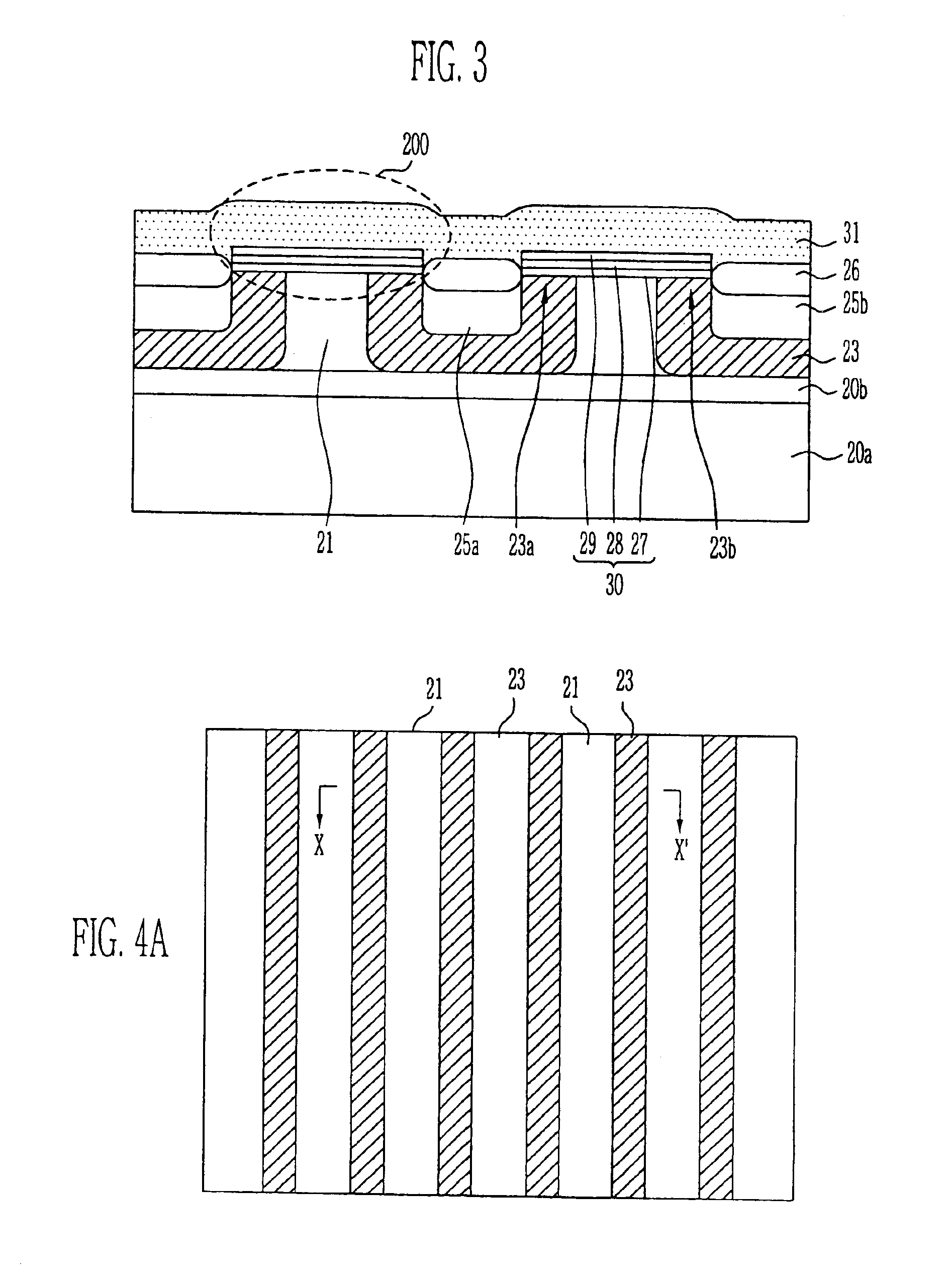
[0040]FIG. 2 is a layout diagram of a flash memory cell according to the present invention and FIG. 3 is a cross-sectional view of the flash memory cell taken along lines X-X′ in FIG. 2.

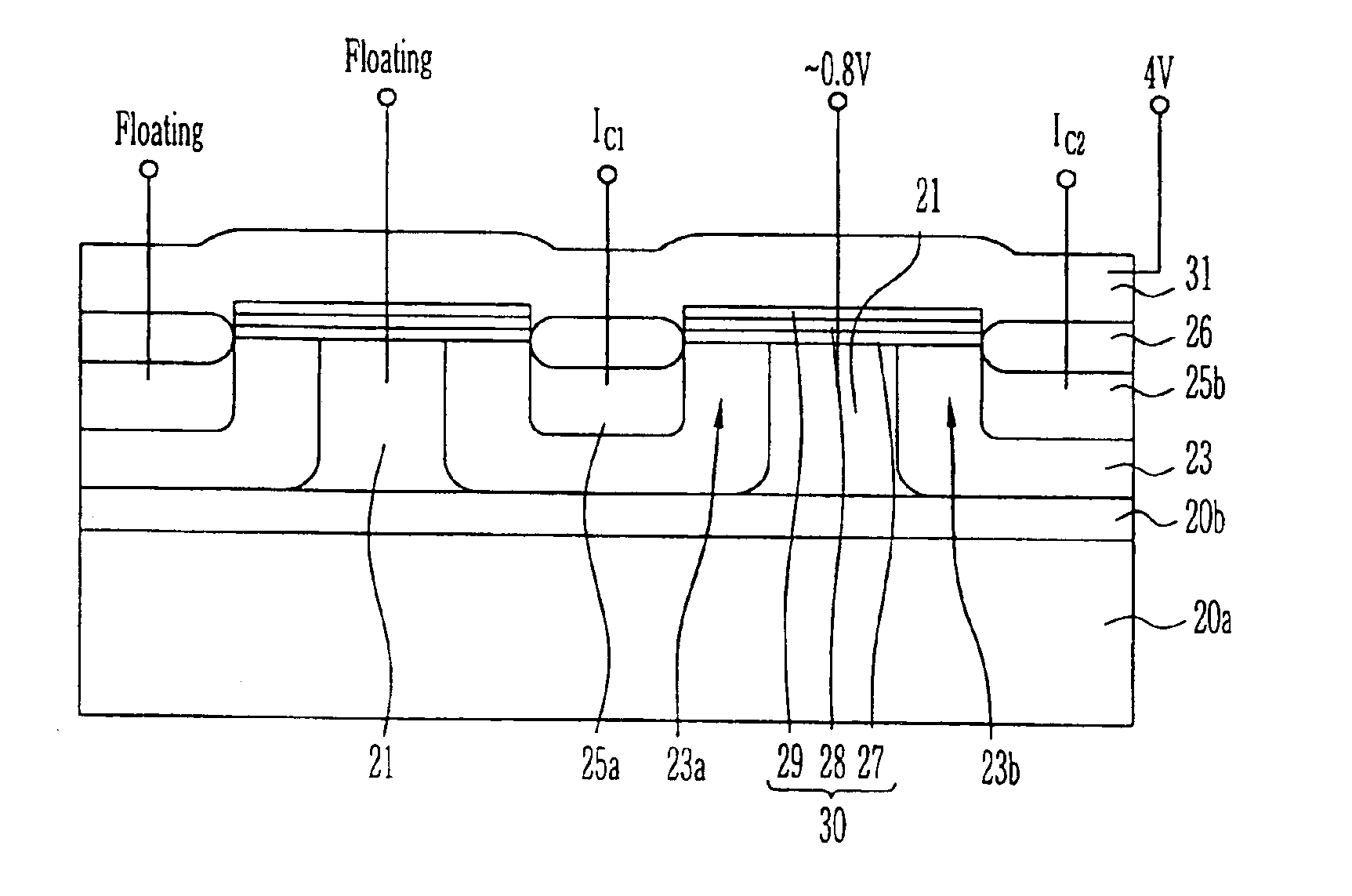
[0041]Referring now to FIGS. 2 and 3, a flash memory cell 200 according to the present invention includes an ONO film 30 formed on a given region of a SOI semiconductor substrate 20, first and second channel regions 23a, 23b formed over the SOI substrate 20 at both edges of the ONO film 30, a source region 21 formed between the first and second channel regions 23a, 23b, first and second drain regions 25a, 25b formed over the SOI substrate 20 at both sides of the ONO film 30, and a word line 31 formed on the ONO film 30.

[0042]The ONO film 30 has a structure in which a lower oxide film 27, a nitr...


PUM


Abstract

The present invention relates to a flash memory cell and method of manufacturing the same, and programming/erasing/reading method in the flash memory cell. According to the present invention, a source region and a drain region are first formed and a tunnel oxide film is then formed. Therefore, it is possible to prevent damage of the tunnel oxide film due to an ion implantation process. Further, independent two channel regions are formed below the floating gate. Thus, it is possible to store data of two or more bits at a single cell. In addition, the tunnel oxide film, the floating gate and the dielectric film having an ONO structure are formed at a given regions. It is thus possible to reduce the steps of a process and improve an electrical characteristic and integration level of a device.

Description

[0001]This application is a division of Ser. No. 10 / 287,781 filed Nov. 5, 2002 and now U.S. Pat No. 6,703,275.BACKGROUND OF THE INVENTION[0002]1. Field of the Invention[0003]The invention relates generally to a flash memory cell and method of manufacturing the same, and programming / erasing / reading method in the flash memory cell. More particularly, the invention relates to a flash memory cell having a silicon-oxide-nitride-oxide-silicon (SONOS) structure in which silicon, an oxide film, a nitride film, an oxide film and silicon are sequentially stacked, and method of manufacturing the same, and programming / erasing / reading method in the flash memory cell.[0004]2. Description of the Prior Art[0005]A flash memory cell is a non-volatile memory device that is electrically programmed and erased. A basic structure and programming / erasing operation of the flash memory cell will be described below.[0006]FIG. 1 is a cross-sectional view of a conventional flash memory cell for describing the s...

Claims


Application Information

Patent Timeline
IPC IPC(8): G11C16/04H01L21/70H01L27/115H01L27/12H01L21/8246H01L21/84G11C16/02H01L21/8247H01L29/788H01L29/792
CPCG11C16/0475H01L21/84H01L27/115H01L27/11568H01L27/1203H10B43/30H10B69/00H01L29/788H10B99/00
Inventor AHN, BYUNG JINPARK, BYUNG SOOCHUNG, SUNG JAE
Owner SK HYNIX INC
Why Eureka
Try Eureka