Process for producing polymer optical waveguide

a polymer and optical waveguide technology, applied in the field of flexible polymer optical waveguides, can solve the problems of poor precision of the resultant core diameter, increased costs, and insufficient refraction index difference, and achieve the effects of reducing the loss of transmission, and reducing the cost of production

Inactive Publication Date: 2005-11-08
FUJIFILM BUSINESS INNOVATION CORP
View PDF9 Cites 6 Cited by
  • Summary
  • Abstract
  • Description
  • Claims
  • Application Information

AI Technical Summary

Benefits of technology

[0020]The present invention has been made in light of the above-described problems and aims to achieve the following. Specifically, it is an object of the invention to provide a process for producing a polymer optical waveguide which can be readily connected to another optical part and achieves remarkably suppressed transmissional loss, in a simple manner and at very low costs.

Problems solved by technology

However, the selective polymerization process (1) has a problem of sticking of the film, and the processes (2) and (3) involve increased costs due to use of photolithography.
The process (4) has a problem of poor precision of the resultant core diameter, and the process (5) has a problem of an insufficient refraction index difference between the core layer and the cladding layer.
Currently, practically employable processes exhibiting superior performance are only the processes (2) and (3), however, these processes are associated with the aforementioned problem of increased costs.
However, this process has a problem in that the polymer precursor material is thinly supplied not only to the capillary groove but also to a space between the pattern substrate and the flat substrate entirely and thereafter cured to form a thin layer having the same composition as the core layer, whereby light leaks out through this thin layer.
However, this method has the following problem: because the monomer is used as the core forming material, the volume shrinkage ratio of the monomer is large when polymerized to form a polymer, and as a result, the transmission loss of the polymer optical waveguide may increase.
This method also has a problem in that due to its complicated procedure, in which the pattern substrate and the flat substrate must be fixed and stuck to each other using the clamp, and fixation at the contact portion must be sealed with the resin, it is impossible to perform mass production using this method and hence cost reduction is unexpected.
Moreover, this method cannot be applied to production of the polymer optical waveguide using, as a clad, a film having a thickness in the order of millimeter or a thickness of 1 mm or less.
However, even if the production process disclosed in this patent is applied to production of the polymer optical waveguide, it takes a prolonged time to form its core portion since the sectional area of the core portion of the polymer optical waveguide is very small, thus making the process unsuitable for mass production.
This process also has a drawback in that when a monomer solution is polymerized to form a polymer, a volume change occurs to alter the shape of the core, whereby the transmission loss increases.
However, even when the optical waveguide is formed by a micromold method, it is impossible to simultaneously fulfil the requirements of reduced volume shrinkage ratio (reduction of transmission loss) occurred when curing and lowered viscosity of a filling liquid (the monomer, etc.) to facilitate the filling.
Accordingly, if reduced transmission loss is preferentially considered, the viscosity of the filling liquid cannot be lowered to a level below a specified limit, whereby the filling speed decreases, and hence the mass production of optical waveguides cannot be expected.
However, this process requires a patterning exposure every time, because of photolithography, when an optical waveguide is formed.
For the foregoing reasons, a problem of increased cost still remains.
In order to three-dimensionally change the sectional area of the optical waveguide in the longitudinal direction, it is necessary to precisely control the depth of the shallow liquid-collecting pool, which poses another problem of a reduced yield.

Method used


Image

  • Process for producing polymer optical waveguide
  • Process for producing polymer optical waveguide
  • Process for producing polymer optical waveguide

Examples


example 1

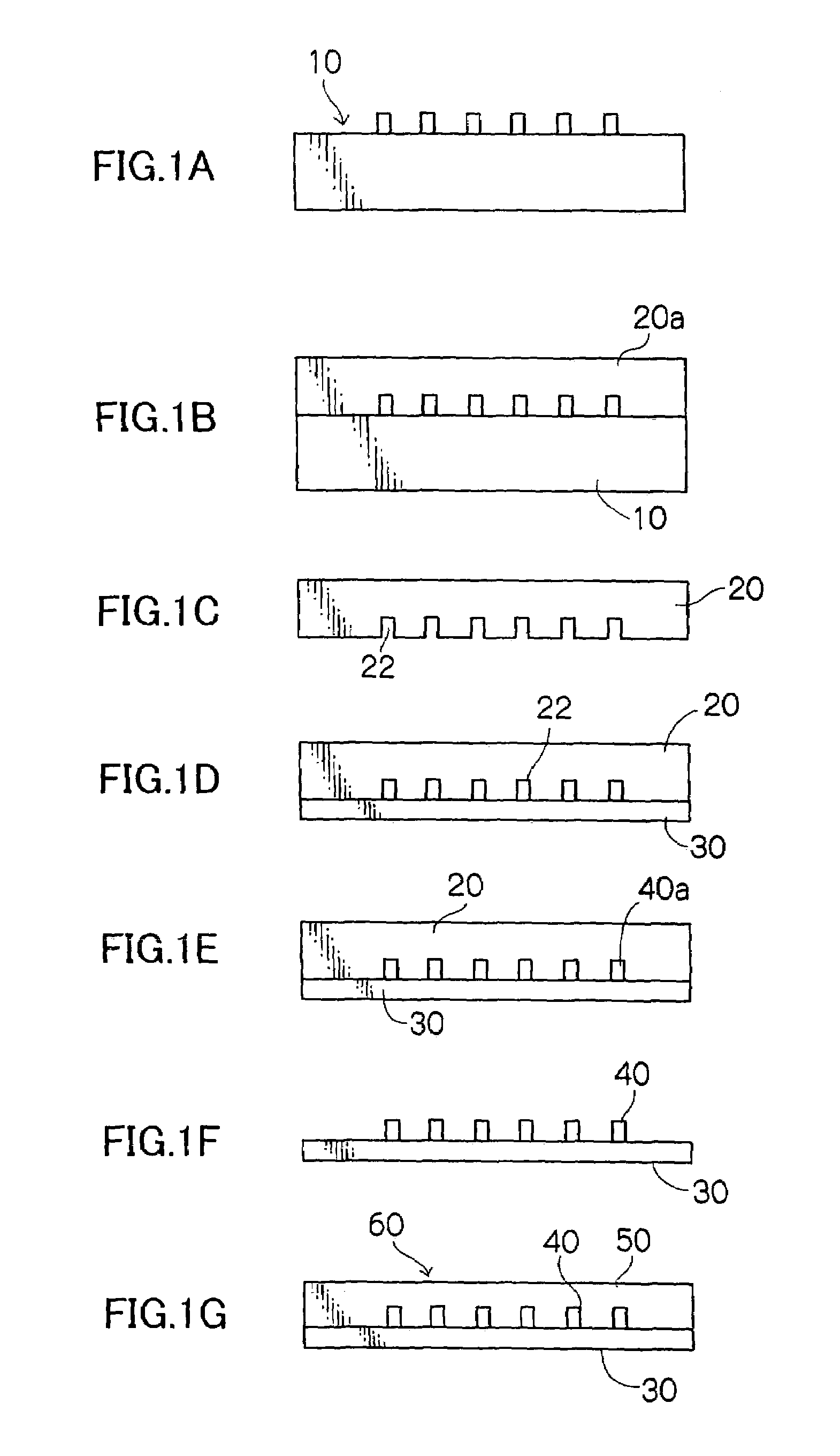
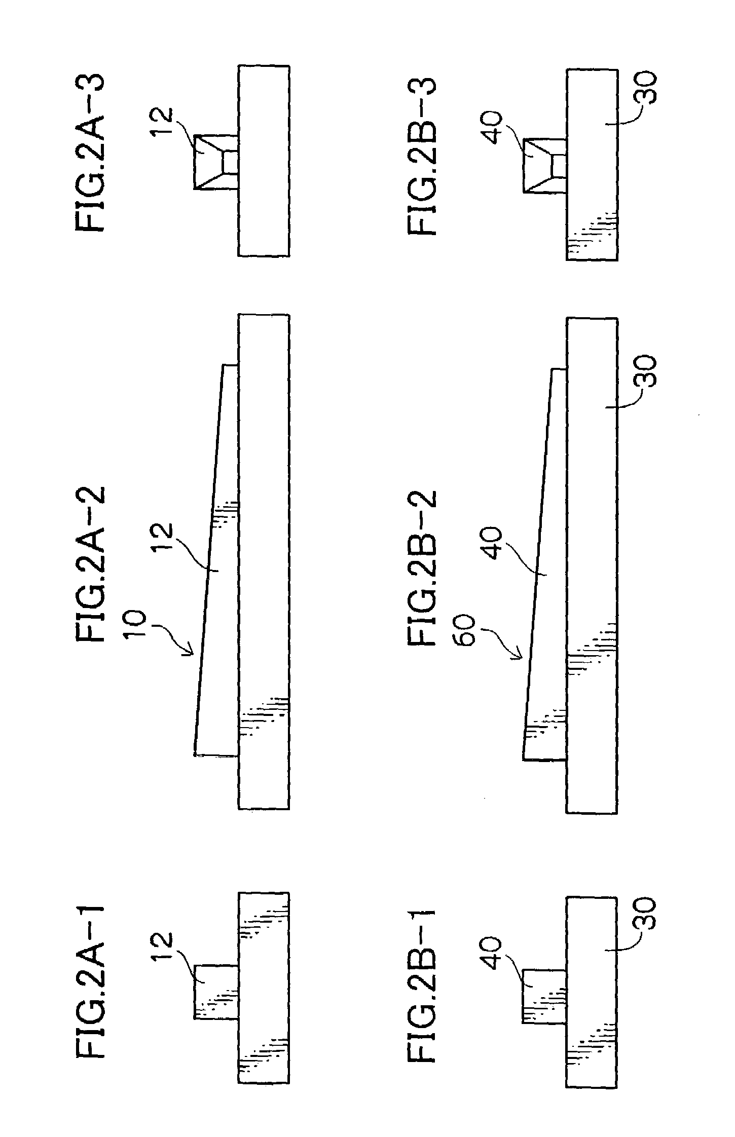
[0120]A quartz glass substrate was subjected to an RIE process to produce a master template having four optical waveguide convex portions, as illustrated in FIGS. 2A-1 to 2A-3. The length of the optical waveguide convex portion was 50 mm, and a sectional shape thereof was a square. A side length of the square of one end face of the convex portion was 80 μm, and another side length of the square of the other end face was 20 μm. The convex portion had a sectional area continuously changing from one end face to the other end face.

[0121]Then, a releasing agent was coated onto this master template, followed by filling a heat-curable dimethylsiloxane resin (SYLGARD 184, manufactured by Dow Corning Asia Co.) thereinto. The filled resin was cured by heating at 120° C. for 30 minutes. Thereafter, the cured resin was peeled to obtain a template (thickness: 3 mm) that had concave portions each having a continuously changing sectional area. Then, both ends of the template was cut to form input ...

example 2

[0125]A master template and a mold were prepared in the same manner as in Example 1, except that the length of optical waveguide convex portions configured in the master template was 50 mm, and a sectional shape thereof (a square) had a side length at one end face of 72 μm and another side length at the other end face of 60 μm.

[0126]This mold was brought close contact with a film (Arton film, manufactured by JSR Corp., refractive index: 1.510) having a larger size than the size of the mold, with a thickness being 188 μm.

[0127]GI type optical fibers each having diameters of 62.5 μm and 50 μm were inserted, by about 1 mm, into a hole made between the mold and the film. Then, several droplets of an UV-curable resin (manufactured by NTT-AT Co.) having a viscosity of 300 mPa·s were supplied into one end of the mold (the end having a larger sectional area of the hole), whereupon the resin was introduced, by capillarity, from the gap between the hole and the optical fibers.

[0128]Subsequent...


PUM

PropertyMeasurementUnit
surface energyaaaaaaaaaa
surface roughnessaaaaaaaaaa
thicknessaaaaaaaaaa

Abstract

A process for producing a polymer optical waveguide including the steps of: preparing a mold by applying a mold-forming resin layer onto a master template, peeling the layer from the master template to obtain a template, and cutting both ends of the template to expose a concave portion; bringing the mold into close contact with a film used for a cladding layer; introducing, by capillarity, a UV-curable resin or heat-curable resin by contacting the resin with one end of the mold; curing the introduced resin and removing the mold from the film; and forming a cladding layer on film on which the core has been formed, wherein a sectional area, a sectional shape, or both of a sectional area and a sectional shape of the core changes in a longitudinal direction of the core, and both end faces of the core have different areas.

Description

BACKGROUND OF THE INVENTION[0001]1. Field of the Invention[0002]The present invention relates to a process for producing an optical waveguide, in particular, a flexible polymer optical waveguide.[0003]2. Description of the Related Art[0004]As the process for producing a polymer optical waveguide, the following processes have been proposed: (1) a process comprising impregnating a film with a monomer, exposing a core portion selectively to light to change a refraction index thereof, and sticking a film thereto (selective polymerization); (2) a process comprising applying a core layer and a cladding layer, and forming a cladding portion by reactive ion etching (RIE); (3) a process employing photolithography to perform exposure and development (direct exposure) using an UV-curable resin obtained by adding a photosensitive material to a polymeric material; (4) a process employing injection molding; (5) a process comprising applying a core layer and a cladding layer, and exposing a core p...

Claims


Application Information

Patent Timeline
Patent Type & Authority Patents(United States)
IPC IPC(8): B29C31/04B29C33/00B29C33/38B29D11/00G02B6/13G02B6/138B29C35/08B29C35/02G02B6/12
CPCB29C31/04B29C33/0016B29C33/3857B29D11/00663G02B6/138B29C35/02B29C2035/0827B29L2011/0075G02B2006/121
Inventor SHIMIZU, KEISHIOHTSU, SHIGEMIYATSUDA, KAZUTOSHIAKUTSU, EIICHI
Owner FUJIFILM BUSINESS INNOVATION CORP
Why Eureka
Try Eureka