Method for room temperature metal direct bonding

a direct bonding and metal technology, applied in the direction of non-electric welding apparatus, manufacturing tools, solid-state devices, etc., can solve the problems of high defect density of hetero-epitaxial grown films, dislocation generation, debonding or cracking, and difficult optimization of process design needed to produce different functions on the same chip containing different materials

Inactive Publication Date: 2005-11-08
INVENSAS BONDING TECH INC
View PDF5 Cites 196 Cited by
  • Summary
  • Abstract
  • Description
  • Claims
  • Application Information

AI Technical Summary

Benefits of technology

[0015]Another object of the present invention is to provide a low or room temperature bonding method by which metallic bonding between wafers or die of semiconductor circuits can be formed in ambient without using external pressure.
[0016]An additional object of the present invention is to provide a low or room temperature bonding method by which metallic bonding of layers of any metal between wafers or die of semiconductor circuits can be formed at room temperature at wafer level in ambient without using external pressure by covering metal layers with a thin film of gold or copper or palladium.
[0018]Another object is to provide a room temperature bonding method by which different substrates or different materials on different substrates with different thermal expansion coefficients can be bonded together without generation of catastrophic stresses between the different substrates or different materials on different substrates.
[0021]A still further object of the present invention is to provide a method and device whereby a reliable mechanical bond can be formed at or near room temperature and a reliable electrical contact can be subsequently formed with a simple low temperature anneal.

Problems solved by technology

To date, such hetero-epitaxial growth has realized a high density of defects in the hetero-epitaxial grown films, largely due to the mismatches in lattice constants between the non-silicon films and the substrate.
However, wafer bonding of dissimilar materials having different thermal expansion coefficients at elevated temperature introduces thermal stresses that lead to dislocation generation, debonding, or cracking.
The design of processes needed to produce different functions on the same chip containing different materials is difficult and hard to optimize.
Indeed, many of the resultant SOC chips (especially those at larger integration size) show a low yield.
However, wafer adhesive bonding usually operates at elevated temperatures and suffers from thermal stress, out-gassing, bubble formation and instability of the adhesive, leading to reduced yield in the process and poor reliability over time.
Very small bonding metal pads can be used resulting in very low parasitics and resulting reduced power and increased bandwidth capability.
Temperature, pressure and low hardness metals are typically employed and usually results in residual stresses.

Method used


Image

  • Method for room temperature metal direct bonding
  • Method for room temperature metal direct bonding
  • Method for room temperature metal direct bonding

Examples


first embodiment

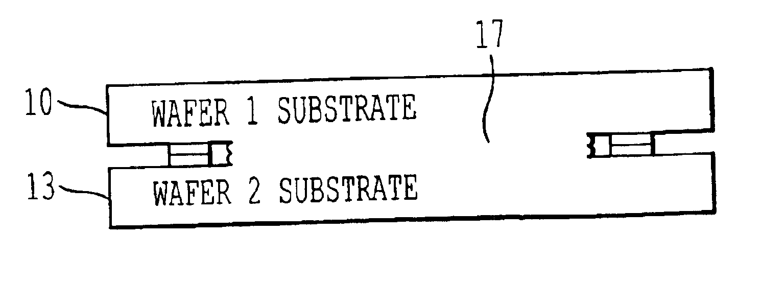
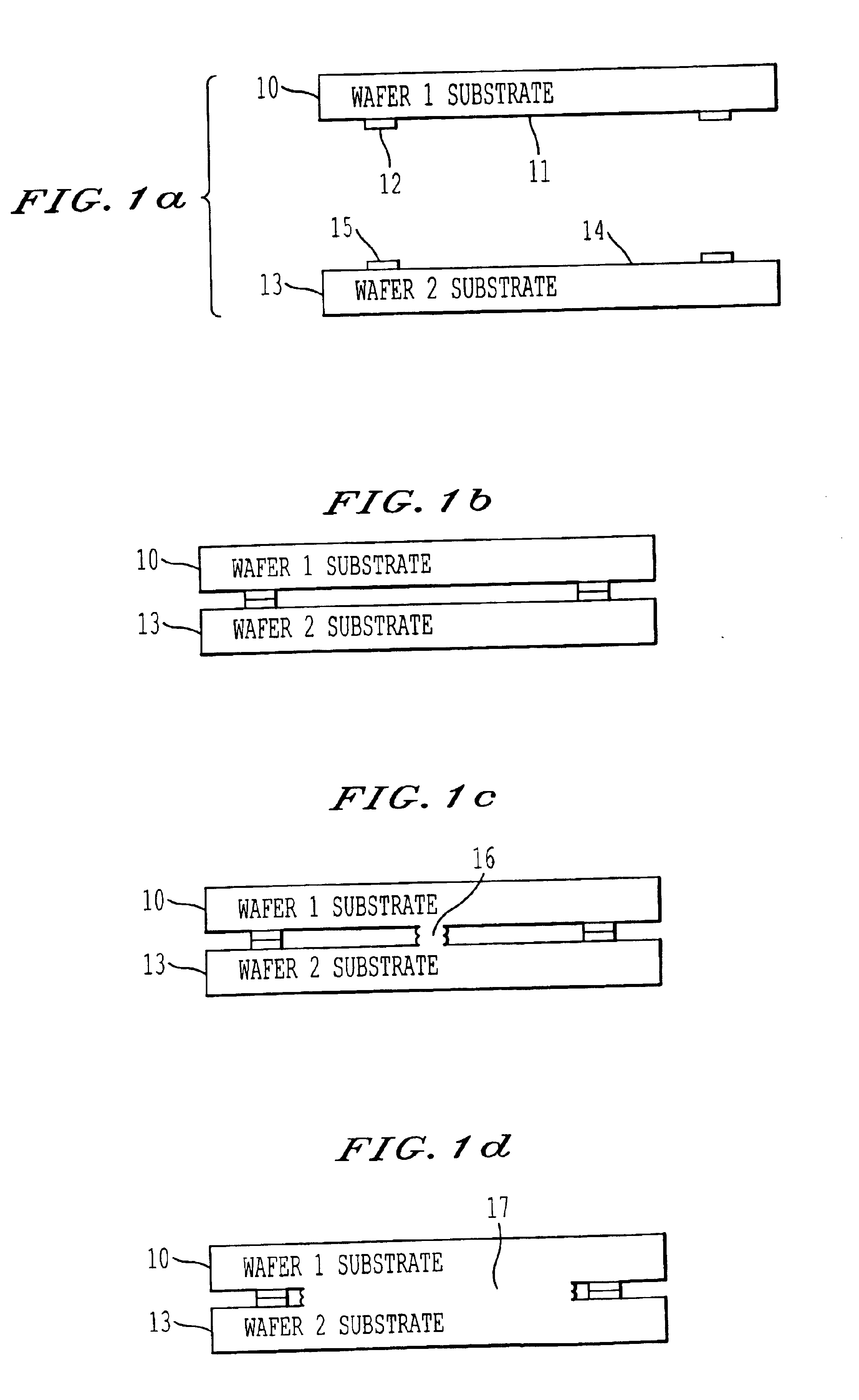
[0057]In one example of the present invention, 5 mm diameter Au bonding pads with a thickness less than 300 Å and a separation distance of 1 mm were deposited on oxide covered 100 mm silicon wafers. Since the Au bonding pads were formed on the surface of the oxide, they also had a height of 300 Angstroms above the surface of the oxide. However, h can be much smaller than actual metal thickness since metal cam be partially buried in oxide or other insulator and h is the height the metal extended above the die surface. A room temperature bonding technology has been developed that cleans and activates the metal and the oxide surfaces compatibly and simultaneously. The Au posts formed a metallic bond by room temperature bonding at wafer level in ambient without using external pressure after storage in air for a period of time, e.g. 60 hr depending on the metal thickness and bonding energy. When the wafer pairs were forcibly separated, by inserting a wedge between the bonded interface, e...

second embodiment

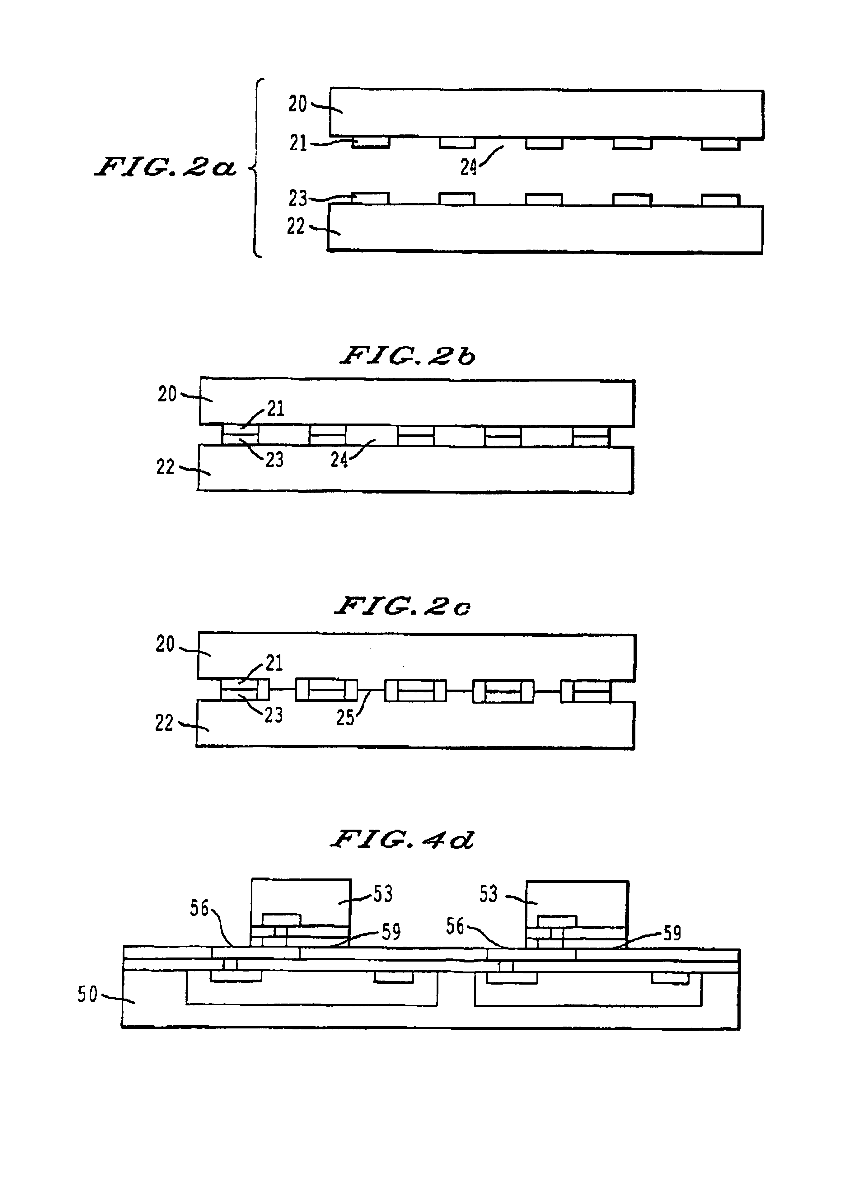
[0059]FIGS. 3A-3C are schematic drawings of a process according to the present invention, by which two different fully processed dies are bonded. The dies are shown to have planar but uneven layer thickness, to demonstrate that the invention may be used in other instances other than even and planar layer thicknesses. In this process, as shown in FIG. 3A, a separate die 30 (only the oxide layer of die 30 is shown, for convenience of explanation) has metal pads 31. The die may be a silicon wafer including semiconductor devices and circuits have opposing surfaces of SiO2. Surface 32 results after a CMP operation.

[0060]As shown in FIG. 3B, vias 36 have been formed and filled with metal to connect with metal pads 31, metal interconnects 33 are formed on wafer 30 to connect with the metal in vias 36, and a layer 34 of thickness t2, of SiO2 or other insulating material is formed on wafer 30. Portions 35 of the SiO2 layer having a width w2 have been removed to expose metal pads 35. The surf...

third embodiment

[0081]the invention allows a significant increase in the metal height above the non-metal surface and / or significant reduction in non-bonded area near the metal while maintaining an acceptable electrical connection between metal portions formed on separate wafers. In this embodiment, deformation of material in the vicinity of the metal material that forms the electrical contact is designed to result from the pressure at the metal surfaces from the wafer-to-wafer chemical bonding of the non-metal portions. This deformation may result in less pressure applied to the metal after the bonding process is complete, but adequate pressure to form an acceptable electrical connection between the metal portions. This deformation allows the gap near the metal surfaces to be significantly reduced or eliminated.

[0082]The object of the deformable material in the vicinity of the metal material forming the electrical contact is to allow the pressure generated by the chemical bonding of the non-metal ...


PUM

PropertyMeasurementUnit
compressive pressureaaaaaaaaaa
pressureaaaaaaaaaa

Abstract

A bonded device structure including a first substrate having a first set of metallic bonding pads, preferably connected to a device or circuit, and having a first non-metallic region adjacent to the metallic bonding pads on the first substrate, a second substrate having a second set of metallic bonding pads aligned with the first set of metallic bonding pads, preferably connected to a device or circuit, and having a second non-metallic region adjacent to the metallic bonding pads on the second substrate, and a contact-bonded interface between the first and second set of metallic bonding pads formed by contact bonding of the first non-metallic region to the second non-metallic region. At least one of the first and second substrates may be elastically deformed.

Description

CROSS-REFERENCE TO RELATED APPLICATIONS[0001]This application is related to application Ser. Nos. 09 / 410,054, 09 / 505,283 and 09 / 532,886, the entire contents of which are incorporated herein by reference.BACKGROUND OF THE INVENTION[0002]1. Field of the Invention[0003]The present invention relates to the field of direct wafer bonding, preferably at room temperature, and more particularly to the bonding of substrates to be utilized in semiconductor device and integrated circuit fabrication.[0004]2. Description of the Related Art[0005]As the physical limits of conventional CMOS device are being approached and the demands for high performance electronic systems are imminent, system-on-a chip (SOC) is becoming a natural solution of the semiconductor industry. For system-on-a chip preparation, a variety of functions are required on a chip. While silicon technology is the mainstay technology for processing a large number devices, many of the desired circuit and optoelectronic functions can ...

Claims


Application Information

Patent Timeline
Patent Type & Authority Patents(United States)
IPC IPC(8): H01L21/70H01L21/98H01L21/60
CPCB23K20/02H01L21/481H01L24/11H01L24/12H01L24/16H01L24/73H01L24/81H01L24/83H01L25/50H01L24/32H01L24/90H01L24/28H01L2224/13099H01L2224/13144H01L2224/13147H01L2224/32145H01L2224/81136H01L2224/81143H01L2224/81193H01L2224/81208H01L2224/8121H01L2224/81815H01L2224/81894H01L2224/8319H01L2224/83801H01L2224/8385H01L2224/83894H01L2224/83907H01L2225/06513H01L2924/01003H01L2924/01005H01L2924/01013H01L2924/01015H01L2924/01018H01L2924/01022H01L2924/01027H01L2924/01029H01L2924/01039H01L2924/01046H01L2924/01047H01L2924/01049H01L2924/0105H01L2924/0106H01L2924/01074H01L2924/01078H01L2924/01079H01L2924/01082H01L2924/01322H01L2924/07802H01L2924/10329H01L2924/14H01L2224/13109H01L2224/9202H01L2924/01006H01L2924/01019H01L2924/01023H01L2924/01033H01L2924/01072H01L2924/01075H01L2924/014H01L2224/13011H01L2924/0132H01L2224/81011H01L2224/81013H01L2224/81014H01L2924/00013H01L2224/8183H01L2224/8383H01L2224/8384H01L2224/81801H01L2224/83095H01L2224/8334H01L2224/83895H01L2924/1532Y10T29/49126H01L2924/1305H01L2924/3512H01L2924/00H01L2224/29099H01L2924/351H01L2924/12042H01L2224/05573H01L2224/05568H01L2224/05571H01L2224/80895H01L2224/80986H01L2224/80035H01L2224/80935H01L24/80H01L24/08H01L2224/08145H01L24/13H01L24/03H01L24/05H01L2224/8034H01L2224/80815H01L2224/80906H01L2224/05644H01L2924/00014H01L2224/05664H01L2224/05669H01L2224/05124H01L2224/05147H01L2224/80896H01L21/44H01L21/48H01L21/50H01L21/76251H01L24/09H01L24/89H01L2224/80801
Inventor TONG, QIN-YIENQUIST, PAUL M.ROSE, ANTHONY SCOT
Owner INVENSAS BONDING TECH INC
Why Eureka
Try Eureka