Semiconductor memory having a pulse generator for generating column pulses

a technology of electromagnetic waves and memory blocks, applied in the field of electromagnetic waves, can solve the problems of high power consumption, high power consumption of read operations, and high power consumption of power supply, and achieve the effect of high speed page operation function, reduced operating power consumption, and high speed operation

Active Publication Date: 2005-11-08
SOCIONEXT INC
View PDF13 Cites 12 Cited by
  • Summary
  • Abstract
  • Description
  • Claims
  • Application Information

AI Technical Summary

Benefits of technology

[0018]It is an object of the present invention to provide a semiconductor memory having a high speed page operat

Problems solved by technology

In the semiconductor memory shown in FIG. 1 a problem arises that activation of all the memory blocks BLK during a read operation increases power consumption.
In

Method used


Image

  • Semiconductor memory having a pulse generator for generating column pulses
  • Semiconductor memory having a pulse generator for generating column pulses
  • Semiconductor memory having a pulse generator for generating column pulses

Examples


first embodiment

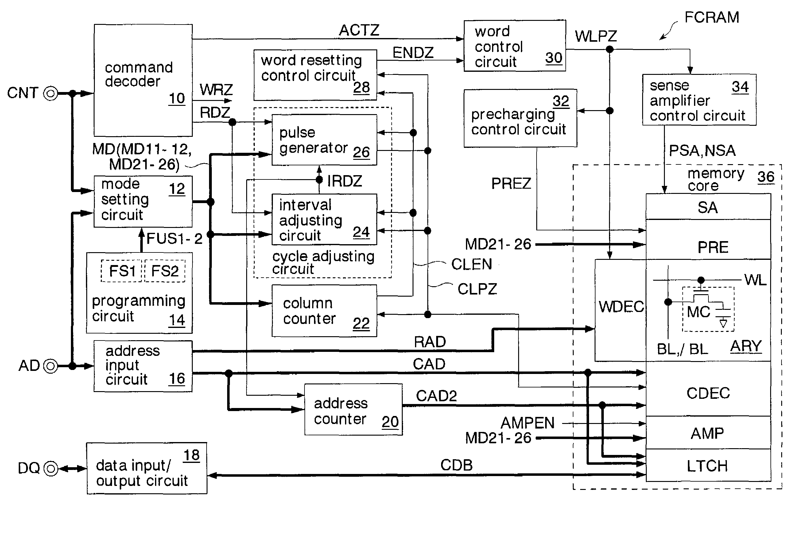
[0077]FIG. 3 shows the semiconductor memory of the present invention. In the diagram, each thick line represents a signal line that consists of a plurality of bits. The double circles shown to the left in the diagram represent external terminals. Signals ending in “Z” are of positive logic. Signals with a leading “ / ” are of negative logic.

[0078]This semiconductor memory is formed as an FCRAM (Fast Cycle RAM) on a silicon substrate by using CMOS processes.

[0079]The FCRAM has a command decoder 10, a mode setting circuit 12, a programming circuit 14, an address input circuit 16, a data input / output circuit 18, an address counter 20, a column counter 22, an interval adjusting circuit 24, a pulse generator 26, a word reset control circuit 28, a word control circuit 30, a precharging control circuit 32, a sense amplifier control circuit 34, and a memory core 36.

[0080]The command decoder 10 decodes a control signal CNT (command signal) which is supplied to a control terminal in order to op...

second embodiment

[0226]The programming circuit 14E has a first switch SW1, a second switch SW2, and a third switch SW3 which are made up of a conductive pattern formed on the semiconductor substrate in conformity to the pattern configuration of a photomask to be used in the semiconductor fabrication processes of the FCRAM. Since the functions of the first switch SW1 and the second switch SW2 are the same as in the second embodiment, description thereof will be omitted here.

[0227]The third switch SW3 outputs a pattern signal PAT3 (third internal setting signal) for indicating the operation mode of the FCRAM (low power mode or high speed mode). That is, the programming circuit 14E outputs the pattern signals PAT1, PAT2, and PAT3 according to the first, second, and third switches SW1, SW2, and SW3 which are set in accordance with the voltages of destinations of the conductive pattern.

[0228]The connection specifications of the first, second, and third switches SW1, SW2, and SW3, or the photomask to be u...


PUM


Abstract

A pulse generator generates a plurality of column pulses in response to a read command. An address counter outputs addresses subsequent to an external address supplied in association with the read command in succession as internal addresses. A column decoder successively selects column selecting lines in synchronization with the column pulses. A plurality of bits of data read from memory cells in response to a single read command RD is successively transmitted to a common data bus line through column switches. This can reduce the number of data bus lines to a minimum, preventing an increase in chip size. Since a single data bus line can transmit a plurality of bits of data, it is possible to minimize the size of the memory region to be activated in response to a read command. This consequently allows a reduction in power consumption.

Description

CROSS REFERENCE TO RELATED APPLICATION[0001]This application is based upon and claims the benefit of priority from Japanese Patent Application No. 2002-251850, filed on Aug. 29, 2002, the entire contents of which are incorporated herein by reference.BACKGROUND OF THE INVENTION[0002]1. Field of the Invention[0003]The present invention relates to a semiconductor memory, and more particularly to a technology for reducing power consumption while maintaining high speed operation.[0004]2. Description of the Related Art[0005]In general, semiconductor memories have a page operation function in which data that is read simultaneously from a plurality of memory cells connected to a word line is output in succession. The page operation function can accelerate operations subsequent to the activation of the memory block, with an improvement in data transfer rate.[0006]For yet improved data transfer rate, there has been recently developed a semiconductor memory which has a high speed page operatio...

Claims


Application Information

Patent Timeline
IPC IPC(8): G11C7/00G11C7/10G11C7/22G11C11/407G11C11/401
CPCG11C7/103G11C7/22G11C7/1048G11C2207/002G11C7/00
Inventor SASAKI, JUNICHISHINOZAKI, NAOHARU
Owner SOCIONEXT INC
Why Eureka
Try Eureka