High-speed and low-power Ti-Ge-Sb nanocomposite phase change thin film and its preparation and application

A nano-composite, low-power technology, applied in the field of materials in the field of microelectronics technology, can solve the problems of alloy thermal stability and crystalline resistivity are not high enough, to achieve fast SET operation speed, fast operation speed, high crystalline resistance Effect

Inactive Publication Date: 2017-11-17
TONGJI UNIV
View PDF2 Cites 12 Cited by
  • Summary
  • Abstract
  • Description
  • Claims
  • Application Information

AI Technical Summary

Problems solved by technology

[0006] The purpose of the present invention is to overcome Ge 8 Sb 92 The shortcomings of the thermal stability and crystalline resistivity of the alloy are not high enough to provide a method that can improve the Ge 8 Sb 92 Thermal stability of phase change material amorphous state, metal element Ti-doped Ge to reduce power consumption of RESET programming 8 Sb 92 Nano phase change thin film material and its preparation and application

Method used


Image

  • High-speed and low-power Ti-Ge-Sb nanocomposite phase change thin film and its preparation and application
  • High-speed and low-power Ti-Ge-Sb nanocomposite phase change thin film and its preparation and application
  • High-speed and low-power Ti-Ge-Sb nanocomposite phase change thin film and its preparation and application

Examples


Embodiment 1

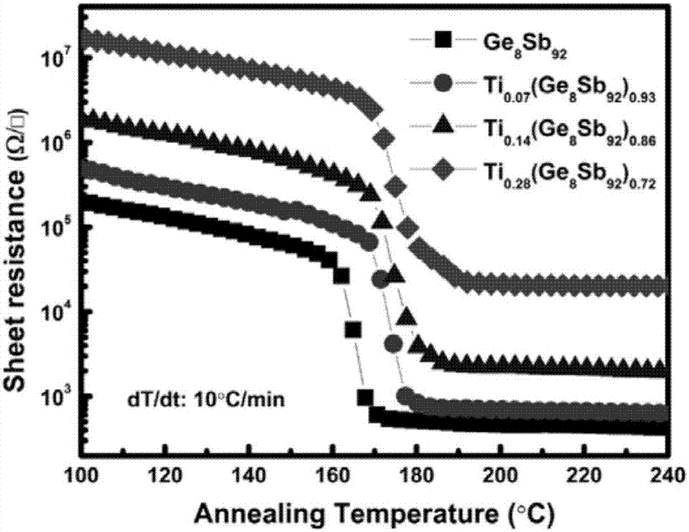
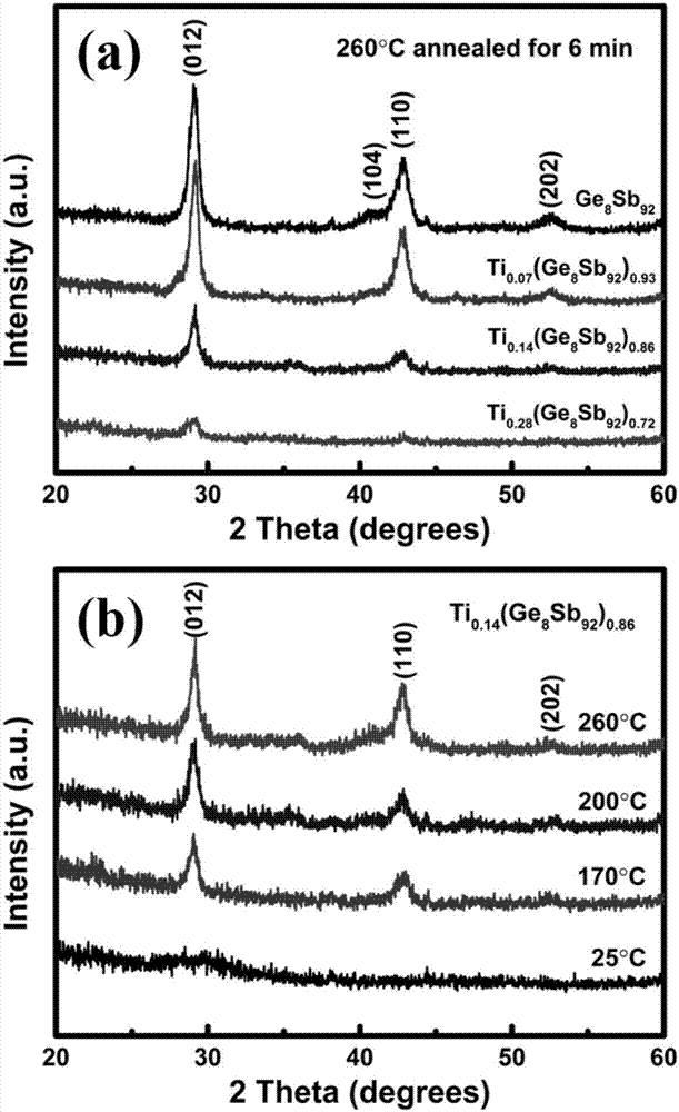
[0041] The present embodiment provides Ti-Ge-Sb nano phase change thin film, and its component is Ti 0.07 (Ge 8 Sb 92 ) 0.93 , the thickness of the film is 50nm.

[0042] The main steps of the main preparation method of the phase change film are as follows:

[0043] 1. Clean SiO2 2 / Si(100) substrate surface and back, remove dust particles, organic and inorganic impurities:

[0044] (a) Place the substrate in an ethanol solution, and clean it ultrasonically for 8 minutes to remove dust particles and inorganic impurities on the surface of the substrate;

[0045] (b) The substrate is placed in an acetone solution, and cleaned by ultrasonic waves for 8 minutes to remove organic impurities on the surface of the substrate;

[0046] (c) Place the substrate in deionized water, clean it with ultrasonic waves for 8 minutes, and clean the surface again;

[0047] (d) Take out the substrate and use high-purity N 2 Blow dry the front and back, and place in a dry box for later use. ...

Embodiment 2

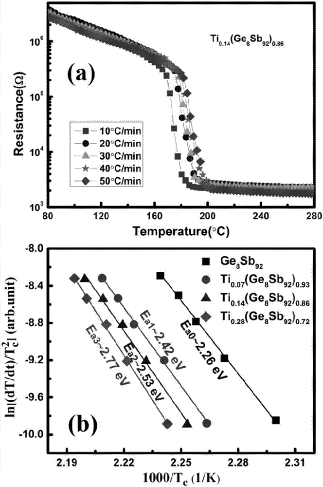
[0057] The present embodiment provides Ti-Ge-Sb nano phase change thin film, and its component is Ti 0.14 (Ge 8 Sb 92 ) 0.86 , the thickness of the film is 50nm.

[0058] The main steps of the main preparation method of the phase change film are as follows:

[0059] 1. Clean SiO2 2 / Si(100) substrate surface and back, remove dust particles, organic and inorganic impurities:

[0060] (a) Place the substrate in an ethanol solution, and clean it ultrasonically for 8 minutes to remove dust particles and inorganic impurities on the surface of the substrate;

[0061] (b) The substrate is placed in an acetone solution, and cleaned by ultrasonic waves for 8 minutes to remove organic impurities on the surface of the substrate;

[0062] (c) Place the substrate in deionized water, clean it with ultrasonic waves for 8 minutes, and clean the surface again;

[0063] (d) Take out the substrate and use high-purity N 2 Blow dry the front and back, and place in a dry box for later use. ...

Embodiment 3

[0073] The present embodiment provides Ti-Ge-Sb nano phase change thin film, and its component is Ti 0.28 (Ge 8 Sb 92 ) 0.72 , the thickness of the film is 50nm.

[0074] The main steps of the main preparation method of the phase change film are as follows:

[0075] 1. Clean SiO2 2 / Si(100) substrate surface and back, remove dust particles, organic and inorganic impurities:

[0076] (a) Place the substrate in an ethanol solution, and clean it ultrasonically for 8 minutes to remove dust particles and inorganic impurities on the surface of the substrate;

[0077] (b) The substrate is placed in an acetone solution, and cleaned by ultrasonic waves for 8 minutes to remove organic impurities on the surface of the substrate;

[0078] (c) Place the substrate in deionized water, clean it with ultrasonic waves for 8 minutes, and clean the surface again;

[0079] (d) Take out the substrate and use high-purity N 2 Blow dry the front and back, and place in a dry box for later use. ...


PUM

PropertyMeasurementUnit
thicknessaaaaaaaaaa
thicknessaaaaaaaaaa
thicknessaaaaaaaaaa

Abstract

The invention relates to a high-speed and low-power Ti-Ge-Sb nanocomposite phase change thin film and its preparation and application. The thin film is a Ge8Sb92 nano phase change thin film doped with a metal element Ti and has a chemical composition conforming to the chemical formula Tix(Ge8Sb92)1-x, where x is the atomic percentage of the metal Ti element and 0<x<0.3. The surface and backside of a SiO2/Si (100) substrate is cleaned firstly to remove dust particles and organic and inorganic impurities during preparation, and then the phase change thin film is prepared by means of magnetron sputtering and co-sputtering. Compared with the prior art, the invention has a faster SET operation speed, a higher crystallization temperature and crystallization activation energy, and a larger crystalline resistance, and facilitates the realization of a high-speed and low-power storage PCRAM.

Description

technical field [0001] The invention relates to materials in the technical field of microelectronics, in particular to a high-speed and low-power consumption Ti-Ge-Sb nanocomposite phase-change film and its preparation and application. Background technique [0002] With the growing market demand for mobile Internet terminals such as tablets and smart phones, the market share of Flash memory has increased year by year, becoming the mainstream non-volatile memory (Non-Volatile Memory, NVM) in the market. Nevertheless, the development of Flash is facing many new challenges. First of all, Flash needs to continuously perform charge injection operations, resulting in a low erasing and writing speed of the device and high power consumption. Secondly, with the development of semiconductor manufacturing technology below 20nm, the charge leakage of Flash devices becomes more and more serious, which brings great unreliability to data storage. For this reason, academia and industry ha...

Claims


Application Information

Patent Timeline
Patent Type & Authority Applications(China)
IPC IPC(8): H01L45/00B82Y30/00
CPCB82Y30/00H10N70/026H10N70/8828
Inventor 翟继卫吴卫华
Owner TONGJI UNIV
Why Eureka
Try Eureka