Substrate, optical fiber connection end member, optical element housing member, and method of fabrication of an optical module and the substrate

a technology of optical modules and housing members, applied in the direction of optical elements, semiconductor lasers, instruments, etc., can solve the problems of high cost, difficult to obtain high precision, and extra space that is necessary in order to achieve the effect of high precision, simple structure and stably realized

Inactive Publication Date: 2005-11-15
NEC CORP
View PDF13 Cites 16 Cited by
  • Summary
  • Abstract
  • Description
  • Claims
  • Application Information

AI Technical Summary

Benefits of technology

[0022]In consideration of the above described problems, it is an object of the present invention to provide an optical waveguide on a substrate or an optical element mounted on a substrate and an optical fiber of an optical fiber connector connected to an optical fiber connecting end member or an optical element provided on an optical element housing member that can be connected without core alignment and at high precision, and furthermore, has a simple structure, and a substrate that can be stably realized, and an optical fiber connecting end member, an optical element housing member, and a fabrication method of an optical module and a substrate.

Problems solved by technology

When an optical module is assembled on the device, an ordinary pigtail module entails the problem of processing of the optical fiber's excess length, which means that extra space is necessary in order to accommodate the optical fiber mounted in the optical module.
However, in this active alignment, because the position adjustment of the optical module and the receptacle must be carried out using a precision manual operation, the optical module becomes a factor that causes a high cost.
However, in the conventional optical waveguide part and the optical waveguide apparatus described above, an optical fiber, which is a very small part, must be aligned with and mounted on a V-shaped groove and an inverse V-shaped groove, and there is the problem that obtaining high precision is difficult.
In addition, the problem with the optical waveguide part and optical waveguide apparatus is the precision of the V-shaped grooves.
This method includes a method of forming a V-shaped groove using machine processing and a method of forming a rectangular groove by etching processing, but generally, in these methods, achieving sub-micron level precision is difficult, and applying these methods to single mode optical fiber arrays presents problems.

Method used


Image

  • Substrate, optical fiber connection end member, optical element housing member, and method of fabrication of an optical module and the substrate
  • Substrate, optical fiber connection end member, optical element housing member, and method of fabrication of an optical module and the substrate
  • Substrate, optical fiber connection end member, optical element housing member, and method of fabrication of an optical module and the substrate

Examples


first embodiment

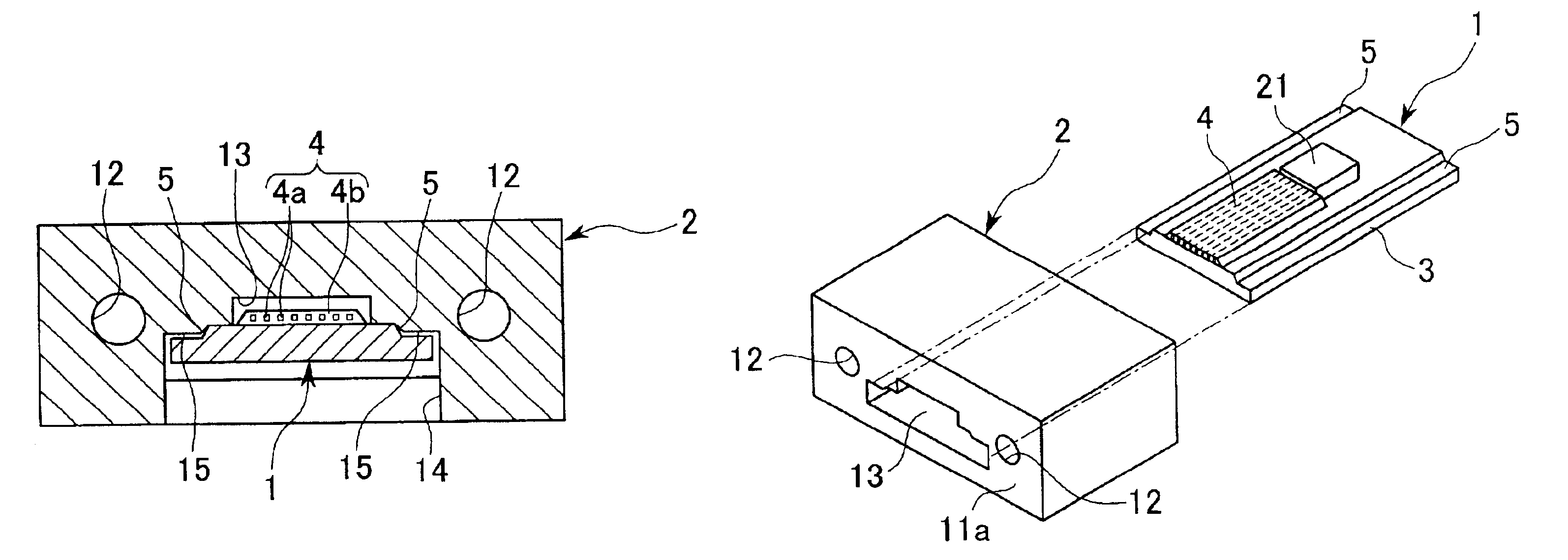
[0055]FIG. 1 is an exploded drawing showing the optical module according to the first embodiment of the present invention, and FIG. 2 is a cross-sectional drawing of the same optical module. In the figures, reference numeral 1 is an optical waveguide substrate (a substrate that provides an optical waveguide), and reference numeral 2 is an optical fiber connecting end member that accommodates and fixes the end of the optical waveguide substrate 1.

[0056]In the optical waveguide substrate 1, a silicon optical waveguide 4, which has a multiple core structure wherein a plurality of cores 4a are buried in the clad 4b, is formed on a rectangular Si substrate 3, and on both sides of the upper surface of this Si substrate 3, high precision steps 5 and 5 are formed along the longitudinal direction thereof by anisotropic etching of the Si.

[0057]One end surface 11a of the plastic housing 11 of the optical fiber connection end member 2 is flattened by grinding, and guide pin insertion holes 12 a...

second embodiment

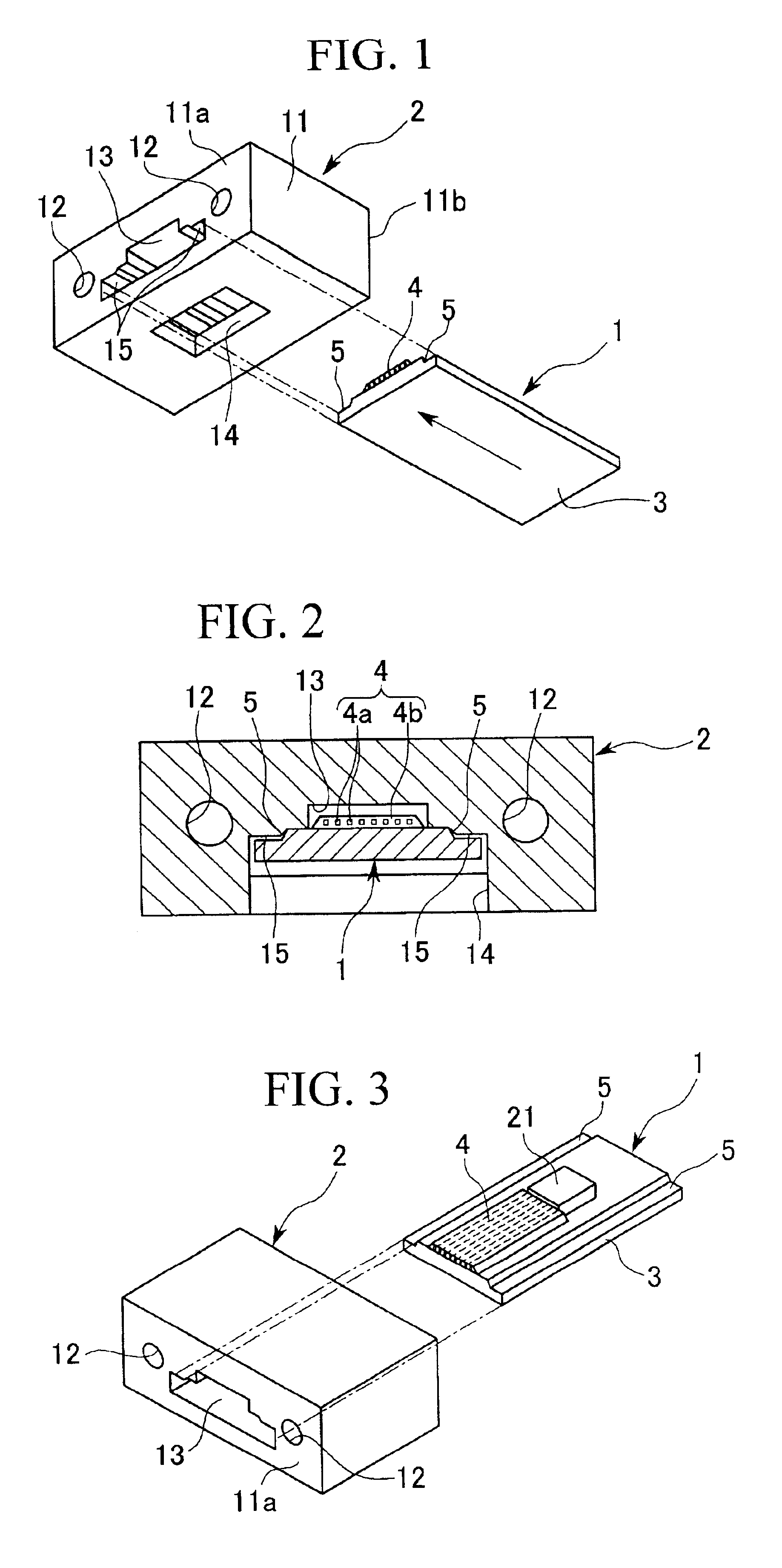
[0063]FIG. 3 is an exploded perspective drawing showing the optical module according to the second embodiment of the present invention, and the point of difference between the optical module according to this embodiment and the optical module according to the first embodiment described above is that, in contrast with the first embodiment in which there is only a structure in which a silicon optical waveguide 4 is formed such that the optical waveguide substrate 1 has a plurality of cores 4a buried in a clad 4b on the Si substrate 3, in the optical module according to the present embodiment, a semiconductor laser (optical element) 21 for inputting a laser beam into the optical waveguide 4 is mounted on the Si substrate 3, thereby making a hybrid light condensing module.

[0064]In this optical module, in addition to the optical waveguide 4, a semiconductor laser 21, which is an optical element, is mounted on the Si substrate 3, and thus the optical module can be hybridized.

third embodiment

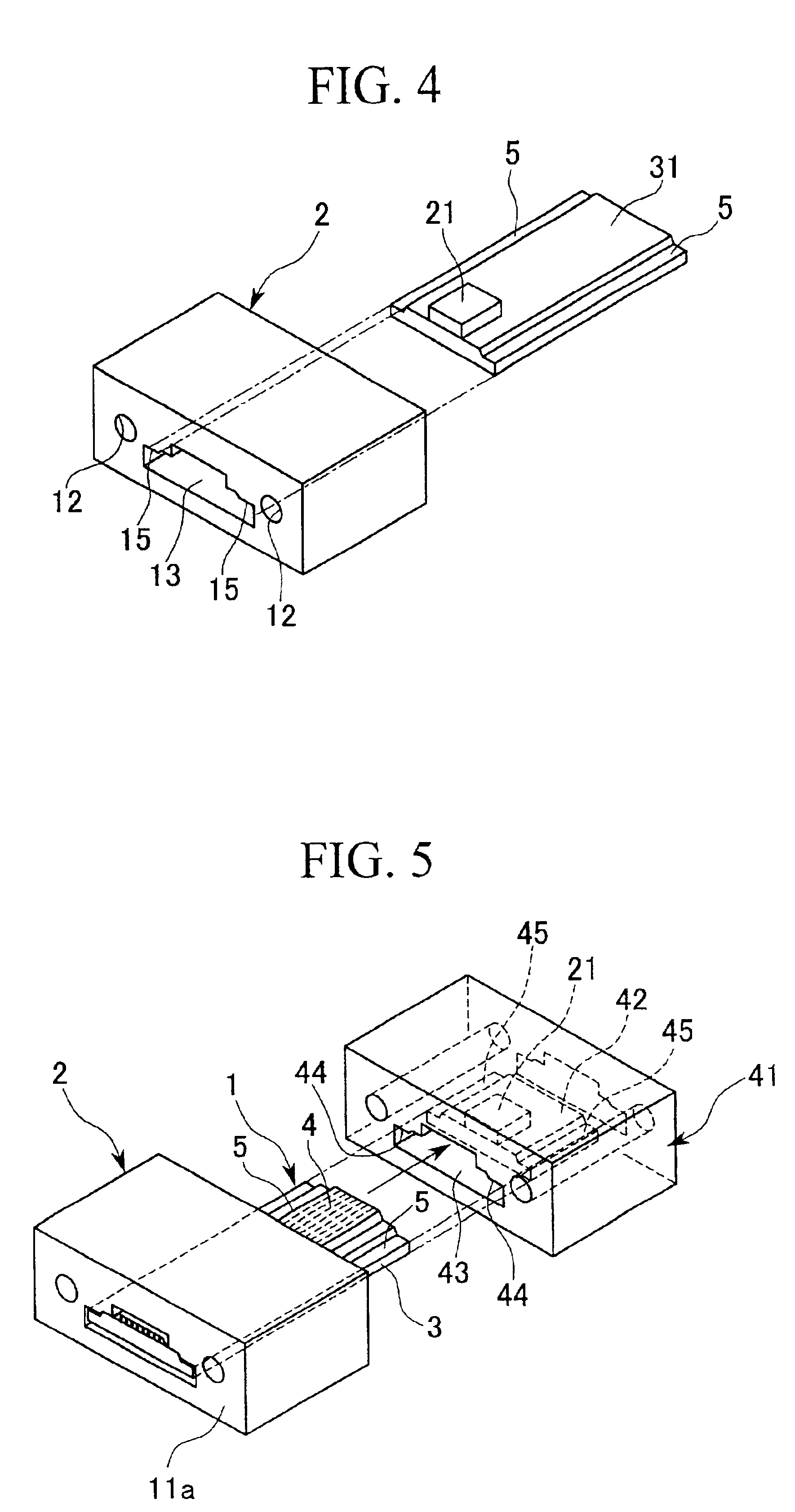
[0065]FIG. 4 is an exploded perspective drawing showing the optical module according to the third embodiment of the present invention, and the point of difference between the optical module according to this embodiment and the optical module according to the first embodiment is that, in contrast to the first embodiment in which there is a structure in which a silicon optical waveguide 4 is formed such that the optical waveguide substrate 1 has a plurality of cores 4a buried in a clad 4b on the Si substrate 3, in the optical module according to the present embodiment, the steps 5 and 5, like those of the first embodiment, are formed using anisotropic etching on both sides of a Si sub-mount (a substrate providing an optical element) 31 on which is mounted a semiconductor laser 21, this Si sub-mount 31 is inserted in the optical fiber connecting end member 2, position alignment is carried out such that the light emitting surface of the semiconductor laser 21 is flush with the end surfa...


PUM


Abstract

The present invention provides a substrate, an optical fiber connecting end member, an optical element-housing member, a light module, and a manufacturing method of the substrate. The substrate has a feature that can be stably realizable and having a simple structure and that a light waveguide formed on the substrate surface or an optical element formed thereon can be connected without core alignment to an optical element provided on the optical fiber of the optical fiber connector to be connected to the optical fiber connecting end member. The substrate of the present invention is characterized in steps 5 for positioning being formed on at least one side of the substrate 1 that provides the optical waveguide 4.

Description

BACKGROUND OF THE INVENTION[0001]1. Field of the Invention[0002]The present invention relates to a substrate, optical fiber connecting terminal member, optical element housing member, and method of fabrication of an optical module and the substrate, and in particular to a substrate, an optical fiber connecting end member, and an optical element housing member that can connect without alignment of the cores and at high precision an optical element mounted on an optical waveguide on a substrate or mounted on the substrate to an optical fiber of an optical fiber connector that is connected to an optical fiber connecting end member or an optical element provided on an optical element housing member, and a fabrication method for an optical module and a substrate.[0003]2. Description of the Related Art[0004]In broadband optical communication networks and high-speed data transmission between computers, parallel optical modules and multiple core optical transmission and reception modules an...

Claims


Application Information

Patent Timeline
Patent Type & Authority Patents(United States)
IPC IPC(8): G02B6/42G02B6/30G02B6/122G02B6/13H01L31/0232H01L33/48H01S5/022
CPCG02B6/30G02B6/423G02B6/4292G02B6/421G02B6/4214G02B6/4246G02B6/4244G02B6/4245G02B6/4257
Inventor SASAKI, JUNICHIKURATA, KAZUHIKOSHIMIZU, TAKANORI
Owner NEC CORP
Why Eureka
Try Eureka