Supercharge Your Innovation With Domain-Expert AI Agents!

Flash NVROM devices with UV charge immunity

a technology of flash nvrom and charge immunity, which is applied in the direction of semiconductor devices, semiconductor/solid-state device details, electrical apparatus, etc., can solve the problems of raising the threshold of the cell so high that it cannot be electrically erased, and achieves the effect of increasing the charge in the layer, improving the yield of flash nvrom memory devices, and raising the threshold of the cell so high

Inactive Publication Date: 2005-11-29
LONGITUDE FLASH MEMORY SOLUTIONS LTD
View PDF11 Cites 13 Cited by
  • Summary
  • Abstract
  • Description
  • Claims
  • Application Information

AI Technical Summary

Benefits of technology

[0008]The present invention generally comprises an NVROM device and its method of fabrication, wherein the UV charge is stored in a nitride layer, and wherein a UV blocking layer overlays the nitride layer. More particularly, the UV blocking layer overlays the control gates which in turn overlay the nitride layer. The UV blocking layer can be inserted in the process flow at different stages of fabrication. The UV blocking layer is preferably formed from a high UV absorption material, such as silicon oxynitride (SiON) or silicon nitride (SiN or Si3N4), a pure stoichiometric material being preferred. In a flash NVROM according to the present invention, exposure of a cell to UV light will not cause the electrons to migrate to a programmed state. Instead, exposure to UV light causes more electrons to collect in the nitride layer, potentially raising the threshold of the cell so high that it cannot be electrically erased. The UV blocking layer prevents UV light from reaching the nitride layer and increasing the charge in the layer.
[0009]Advantages of the present invention include improving yields for flash NVROM memory devices, improving reliability of programmed NVROM devices, and improving memory retention in the cells of flash NVROM devices. Further advantages of the present invention will be explicated in the following portions of the specification, wherein the detailed description is for the purpose of fully disclosing preferred embodiments of the invention without thereon placing limitations.

Problems solved by technology

Instead, exposure to UV light causes more electrons to collect in the nitride layer, potentially raising the threshold of the cell so high that it cannot be electrically erased.

Method used


Image

  • Flash NVROM devices with UV charge immunity
  • Flash NVROM devices with UV charge immunity
  • Flash NVROM devices with UV charge immunity

Examples


Embodiment Construction

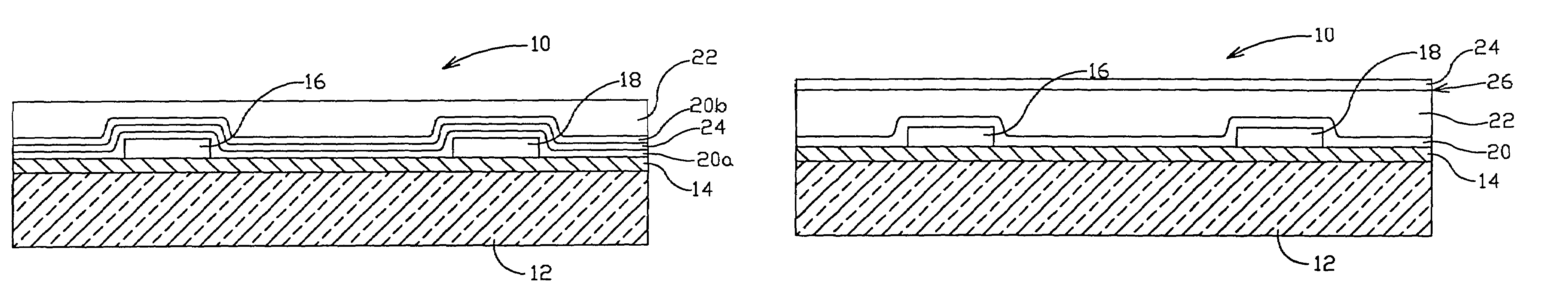
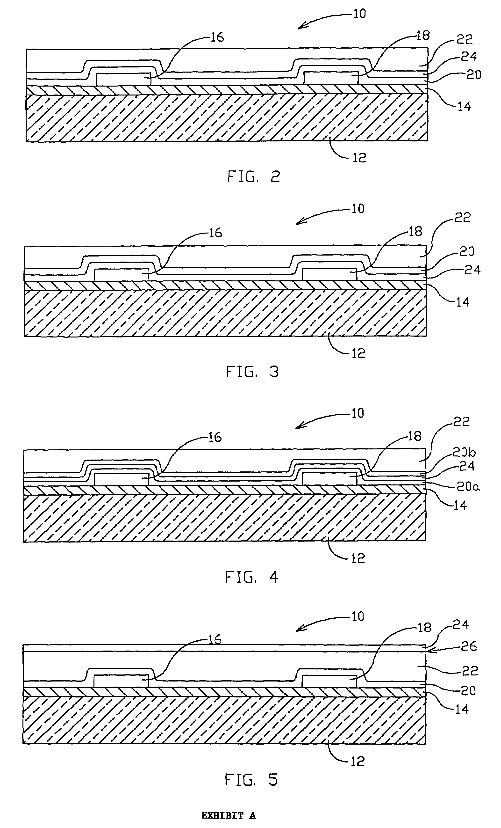
[0016]Referring more specifically to the drawings, for illustrative purposes, the present invention is embodied in the apparatus therein generally shown and the fabrication method described in connection therewith. The apparatus may also vary as to both configuration and to details. The method may also vary as to the specific steps and sequence without departing from the basic concepts as herein disclosed.

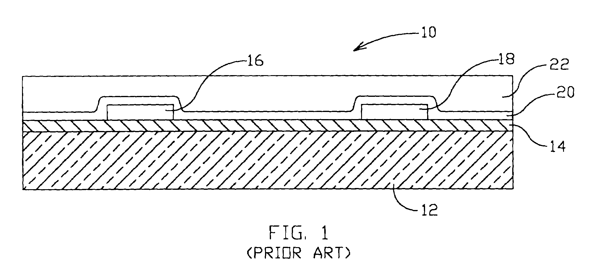
[0017]Referring first to FIG. 1, an example of a conventional two cell NVROM device 10 is shown in accordance with the prior art. In the example shown, the device comprises a substrate layer 12, a floating gate comprising an oxide-nitride-oxide (ONO) dielectric layer 14 overlying the substrate layer, a pair of control gates 16 and 18 overlying the ONO layer, a high temperature oxide (HTO) layer 20 overlying and surrounding control gates 16 and 18, and a borophosphosilicate glass (BPSG) interlayer dielectric (ILD) layer 22 overlaying the HTO layer. In such a device, the nitride laye...


PUM


Abstract

A method of preventing UV charging of flash NVROM cells during fabrication and a device thereby formed. During device fabrication, a UV blocking layer is deposited over the floating gates. The UV blocking layer substantially blocks UV from entering the gate regions so as to prevent electron mobility sufficient to render the cells unprogrammable or unerasable. The reduced electron migration during processing of the NVROM leads to increased yield and reliability of the devices.

Description

CROSS-REFERENCE TO RELATED APPLICATION(S)[0001]This application claims priority from U.S. Provisional Application Ser. No. 60 / 212,618 filed Jun. 19, 2000.FIELD OF THE INVENTION[0002]This invention pertains generally to read-only memory (ROM) devices and fabrication techniques, and more particularly to preventing electrons in the floating gate of a flash non-volatile read only memory (NVROM) device from being affected by ultraviolet light (UV) exposure during fabrication.BACKGROUND OF THE INVENTION[0003]In recent years, the use of solid-state memory devices as a form of data storage media in computer and other electronic equipment has become widespread. For example, programmable ROMs (PROMs), which are non-volatile, are often used for storing data or programs which do not change frequently and which must survive when power is removed from the memory.[0004]All PROM's can be programmed at least once. However, there are also types of PROMs that can be erased. For example, flash non-vola...

Claims


Application Information

Patent Timeline
IPC IPC(8): H01L21/28H01L21/336H01L21/8246H01L23/552H01L27/115
CPCH01L21/28273H01L23/552H01L27/115H01L27/11568H01L2924/0002H01L2924/00H01L29/40114H10B43/30H10B69/00
Inventor PHAM, TUAN DUCRAMSBEY, MARK T.SHIELDS, JEFFREY A.HUI, ANGELA T.HOPPER, DAWN
Owner LONGITUDE FLASH MEMORY SOLUTIONS LTD
Features
  • R&D
  • Intellectual Property
  • Life Sciences
  • Materials
  • Tech Scout
  • Unparalleled Data Quality
  • Higher Quality Content
  • 60% Fewer Hallucinations
Learn More