Image sensor with light guides

a technology of image sensor and light guide, which is applied in the direction of optical elements, radio frequency control devices, instruments, etc., can solve the problems of black and white sensor image resolution degradation, color sensor limitation, and difficult material selection, so as to reduce crosstalk

Active Publication Date: 2005-11-29
TAIWAN SEMICON MFG CO LTD
View PDF15 Cites 83 Cited by
  • Summary
  • Abstract
  • Description
  • Claims
  • Application Information

AI Technical Summary

Benefits of technology

[0018]In order to achieve these objects, the present invention provides an image sensor device. An image sensing array is formed in a substrate, wherein the image sensing array comprises a plurality of photosensors with spaces therebetween. A first dielectric layer is formed overlying the spaces but not the photosensors. A conformal second dielectric layer is formed on a sidewall of the first dielectric layer, wherein the second dielectric layer has a second refractive index. A third dielectric layer is formed overlying the photosensors but not the spaces, wherein the third dielectric layer has a third refractive index. The third refractive index is greater than the second refractive index. A light guide constructed by the second and third dielectric layers is formed overlying each photosensor, thereby preventing incident light from striking other photosensors.
[0019]The present invention also provides a method of forming an image sensor device. An image sensing array is formed in a substrate, wherein the image sensing array comprises a plurality of photosensors with spaces therebetween. A first dielectric layer of a multi-dielectric structure is formed overlying the photosensors and the spaces. The first dielectric layer is patterned by removing part of the first dielectric layer to form an opening above each photosensor while maintaining the first dielectric layer overlying the spaces. A dielectric layer is formed on the first dielectric layer and an inner surface of the opening. Part of the dielectric layer is anisotropically etched back to form a conformal second dielectric layer on the sidewall of the opening, wherein the second dielectric layer has a second refractive index. A third dielectric layer is formed overlying the first dielectric layer, the second dielectric layer and the opening, wherein the third dielectric layer has a third refractive index. Part of the third dielectric layer is removed to the first dielectric layer while maintaining the third dielectric layer in the opening. The third refractive index is greater than the second refractive index. Thus, a light guide comprising the second dielectric layer and the third dielectric layer is formed overlying each photosensor, thereby preventing incident light from striking other photosensors.
[0020]The present invention improves on the prior art in that the image sensor device has a light guide comprising the second dielectric layer and the third dielectric layer overlying each photosensor. Thus, the light guide prevents incident light from striking other photosensors. In addition, the material selection for the IMD layer is less limited as there is no relation between the first dielectric layer and the third dielectric layer. The light guide of the present invention can avoid light scattering between adjacent pixels, thereby reducing crosstalk and ameliorating the disadvantages of the prior art.

Problems solved by technology

The light scattering problem causes degraded image resolution for black and white sensors or complicated color correction for color sensors.
Use of metal shields, however, requires that the metal lines 60 and 62 be isolated, and this limitation requires increased pixel size.
Moreover, when an IMD layer having multi-dielectric films (e.g. SiON, FSG and SiN) is utilized, the material selection is more difficult.
Nevertheless, this method does not disclose a light guide in the dielectric layers.
Nevertheless, this method does not disclose a light guide for an image sensor.

Method used


Image

  • Image sensor with light guides
  • Image sensor with light guides
  • Image sensor with light guides

Examples


Embodiment Construction

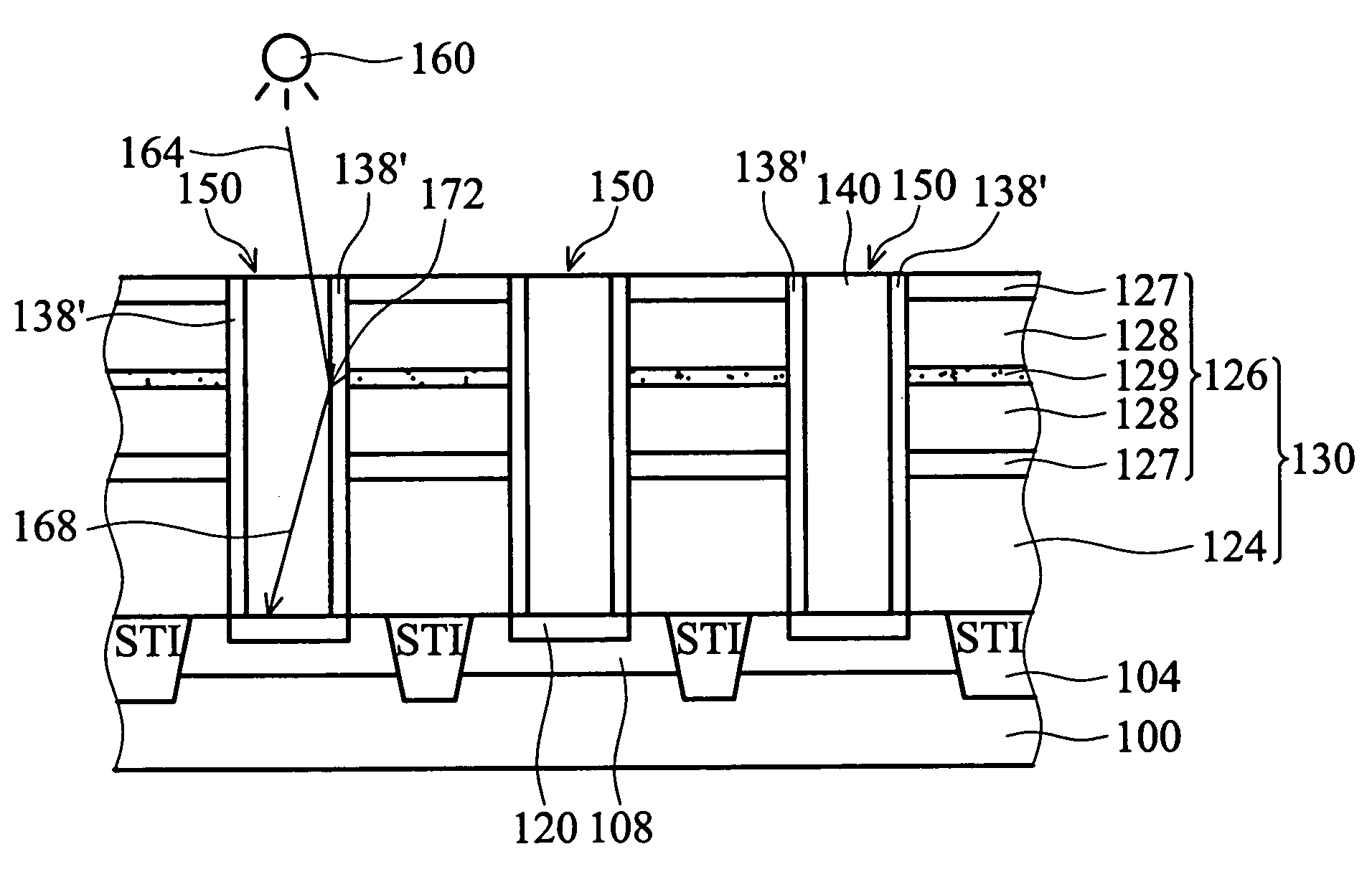
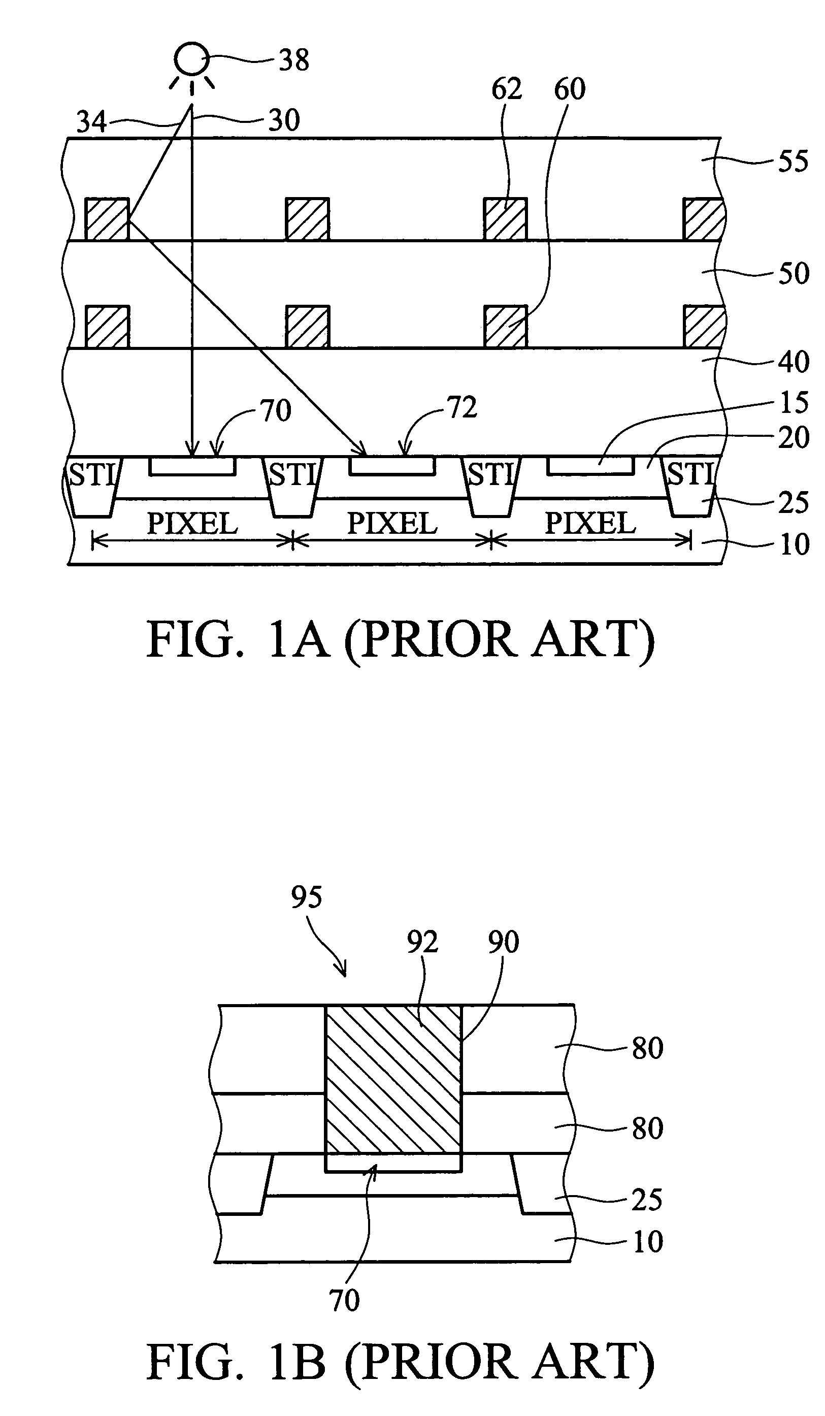
[0026]The present invention provides an image sensor device and fabrication method thereof. The image sensor device is very suitable for a solid state image sensor, such as a CCD (charge-coupled device) or a CMOS (complementary metal-oxide semiconductor) imager. In order to simplify the illustration, a representative photodiode array serving as a photosensor array is illustrated in the preferred embodiment of the present invention; the peripheral regions of the image sensor device are not illustrated.

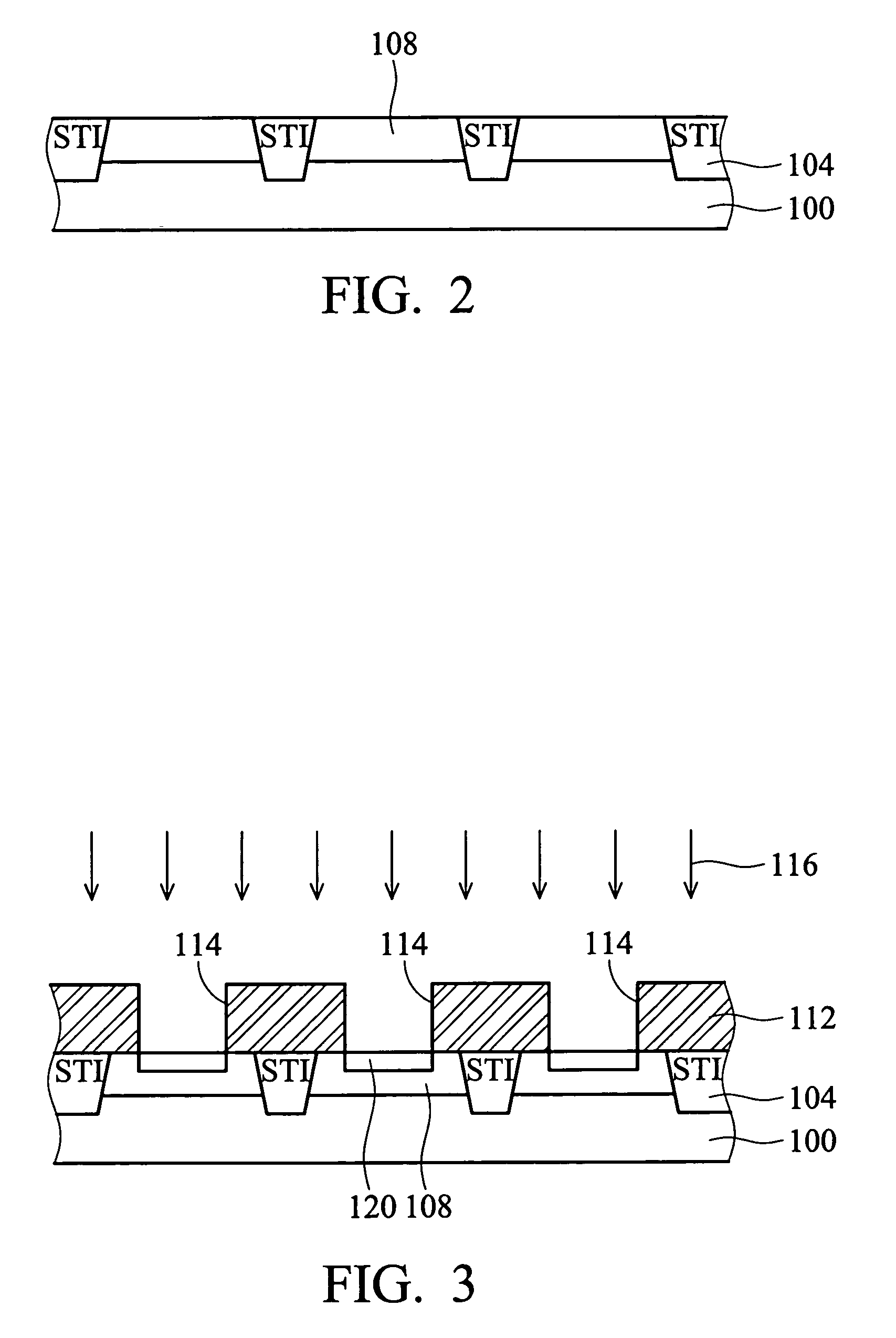
[0027]FIGS. 2˜9 illustrate a process of manufacturing a modified image sensor device of the present invention. FIG. 10 illustrates the improved performance of the preferred embodiment of the present invention. Several important features of the present invention are shown therein and discussed below. The embodiments of the present invention are applied to the formation of a unique, image sensor array comprising a plurality of photodiodes (i.e. photosensors) formed in a semiconductor subs...


PUM


Abstract

An image sensor device and fabrication method thereof. An image sensing array is formed in a substrate, wherein the image sensing array comprises a plurality of photosensors with spaces therebetween. A first dielectric layer with a first refractive index is formed overlying the spaces but not the photosensors. A conformal second dielectric layer with a second refractive index is formed on a sidewall of the first dielectric layer. A third dielectric layer with a third refractive index is formed overlying the photosensors but not the spaces. The third refractive index is greater than the second refractive index. A light guide constructed by the second and third dielectric layers is formed overlying each photosensor, thereby preventing incident light from striking other photosensors.

Description

BACKGROUND OF THE INVENTION[0001]1. Field of the Invention[0002]The present invention relates to a method of forming an image sensor device, and more particularly, to a method of forming light guides of an image sensor device to eliminate crosstalk between pixels.[0003]2. Description of the Related Art[0004]Light imaging array devices are used in a wide variety of applications. These devices utilize an array of active pixels or image sensor cells, comprised with photodiode elements, to collect photon energy to convert images into streams of digital data.[0005]In FIG. 1A, a traditional image sensor device is illustrated in cross section. The device comprises a semiconductor substrate 10 having an array of photodiodes formed therein. Each photodiode comprises, for example, an n-type region 15 in a p-type region 20. Each photodiode is separated from other photodiodes by an array of isolation structures 25, such as shallow trench isolation (STI). Thus, an array of pixels is obtained. Th...

Claims


Application Information

Patent Timeline
Patent Type & Authority Patents(United States)
IPC IPC(8): G02B6/00H01L21/00H01L27/146H01L31/00H01L31/0232
CPCH01L27/1462H01L27/14623H01L27/14625H01L27/14685
Inventor YAUNG, DUN-NIANYU, CHUNG-YI
Owner TAIWAN SEMICON MFG CO LTD
Why Eureka
Try Eureka