Liquid crystal display device and method of fabricating the same

Inactive Publication Date: 2005-11-29
LG DISPLAY CO LTD
View PDF12 Cites 18 Cited by
  • Summary
  • Abstract
  • Description
  • Claims
  • Application Information

AI Technical Summary

Benefits of technology

[0017]To achieve these and other advantages and in accordance with the purpose of the present invention, as embodied and broadly described, a thickness and a dielectric constant of the organic insulating film are set such that a signal delay at the gate line and the data line is reduced.
[0018]In another aspect of the present invention, a thickness of the organic insulating film is set such that an open circuit and a poor contact between a source electrode of the thin film transistor and the pixel electrode can be prevented.
[0019]According to still another aspect of the present invention, a thickness of the organic insulating film is set within a range of 0.8 to 1.5 μm such that an open circuit and a poor contact between a source electrode of the thin film transistor and the pixel electrode can be p

Problems solved by technology

Accordingly, the LCD has low picture brightness as well as a large power consumed in the back light.
But the organic protective film 28 has a problem in that it generates a high parasitic capacitance at an overlapping area between the pixel electrode 20 and the data line 22, or the pixel electrode 20 and the gate electrode 24 because its thickness is small.
As a result, a picture is distorted such that a desired color signal can not be expressed.
However, a rotation speed (RPM) at the time of the spin coating is lowered when a thickness of the organic protective film 28 i

Method used


Image

  • Liquid crystal display device and method of fabricating the same
  • Liquid crystal display device and method of fabricating the same
  • Liquid crystal display device and method of fabricating the same

Examples


Embodiment Construction

[0034]Reference will now be made in detail to the preferred embodiment of the present invention, an example of which is illustrated in the accompanying drawings.

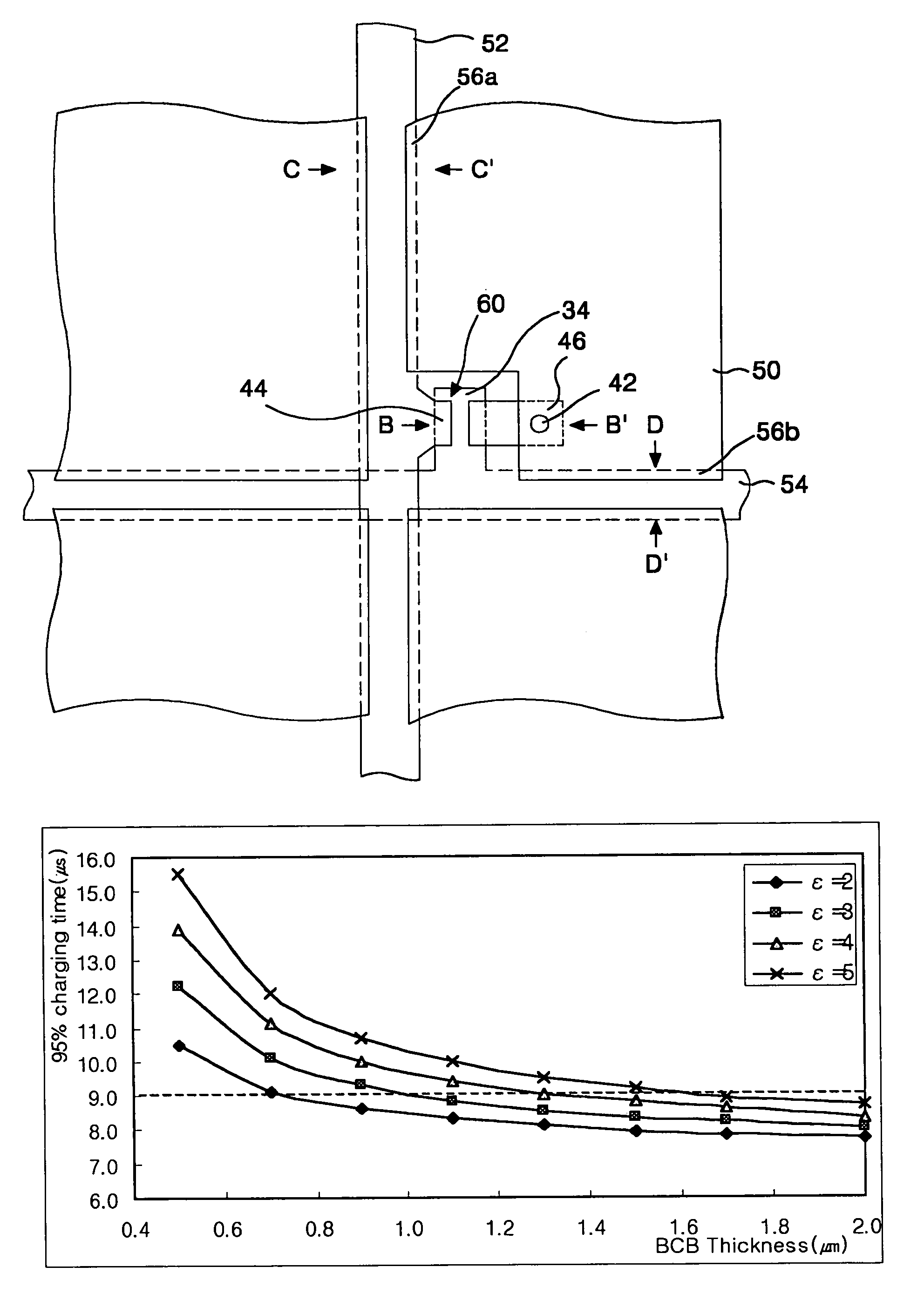
[0035]Referring to FIG. 4, there is shown a liquid crystal display device with a repair function according to a preferred embodiment. In the liquid crystal display device, a TFT 60 is formed at an intersection between a data line 52 and a gate line 54, and pixel electrodes 50 overlapping with the data line 52 and the gate line 54 are arranged in a matrix pattern. The data line 52 applies a video signal to each liquid crystal pixel cell. The gate line 54 applies a gate pulse synchronized with the video signal to a gate electrode 34 of the TFT 60. Each liquid crystal pixel cell includes a liquid crystal layer injected between the pixel electrode 50 and a common electrode (not shown). The liquid crystal layer is driven with an electric field between the pixel electrode 50 and the common electrode to control a transmitted light ...


PUM


Abstract

A liquid crystal display device and a method of fabricating the same that is capable of speeding up a data charge time in a liquid crystal pixel cell in a liquid crystal display device with a high aperture ratio overlapping a pixel electrode and a signal wiring. In the device, a thickness and a dielectric constant of the organic insulating film are set such that a signal delay at the gate line and the data line can be reduced.

Description

[0001]This application claims the benefit of Korean Patent Application No. 1999-44791, filed on Oct. 15, 1999, which is hereby incorporated by reference for all purposes as if fully set forth herein.BACKGROUND OF THE INVENTION[0002]1. Field of the Invention[0003]The present invention relates to a liquid crystal display device, and more particularly to a liquid crystal display device with a high aperture ratio having pixel electrodes overlapped with signal wiring that is capable of speeding up the data charging time of liquid crystal pixel cells. The present invention also is directed to a method of fabricating such a liquid crystal display device.[0004]2. Discussion of the Related Art[0005]Generally, an active matrix liquid crystal display (LCD) driving system displays a natural moving picture by employing thin film transistors (TFTs) as a switching device. Such a liquid crystal display has been commercially available for a monitor for a portable television and a lap-top type person...

Claims


Application Information

Patent Timeline
IPC IPC(8): G02F1/136G02F1/1333G02F1/1362G02F1/1368G09F9/30H01L29/786
CPCG02F1/136227G02F1/1333
Inventor PARK, KWANG SEOPKWAK, DONG YEUNGCHUNG, JAE YOUNG
Owner LG DISPLAY CO LTD
Why Eureka
Try Eureka