

Dual gated finfet gain cell
a gain cell and dual gate technology, applied in the field of memory gain cells and memory circuits, can solve the problems of limiting cell density, consuming large areas on the substrate surface, and increasing the cost of sram cells to produce,
- Summary
- Abstract
- Description
- Claims
- Application Information
AI Technical Summary
Benefits of technology
Problems solved by technology
Method used
Image

Examples
Embodiment Construction
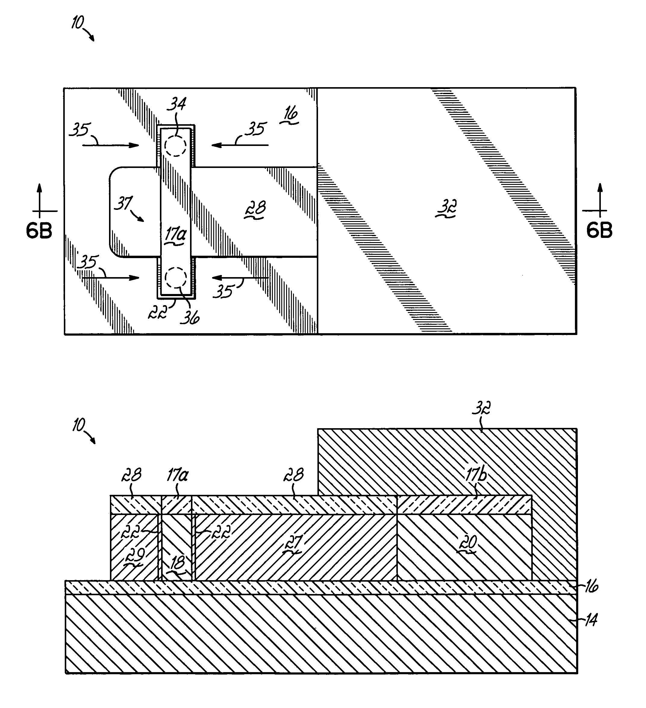
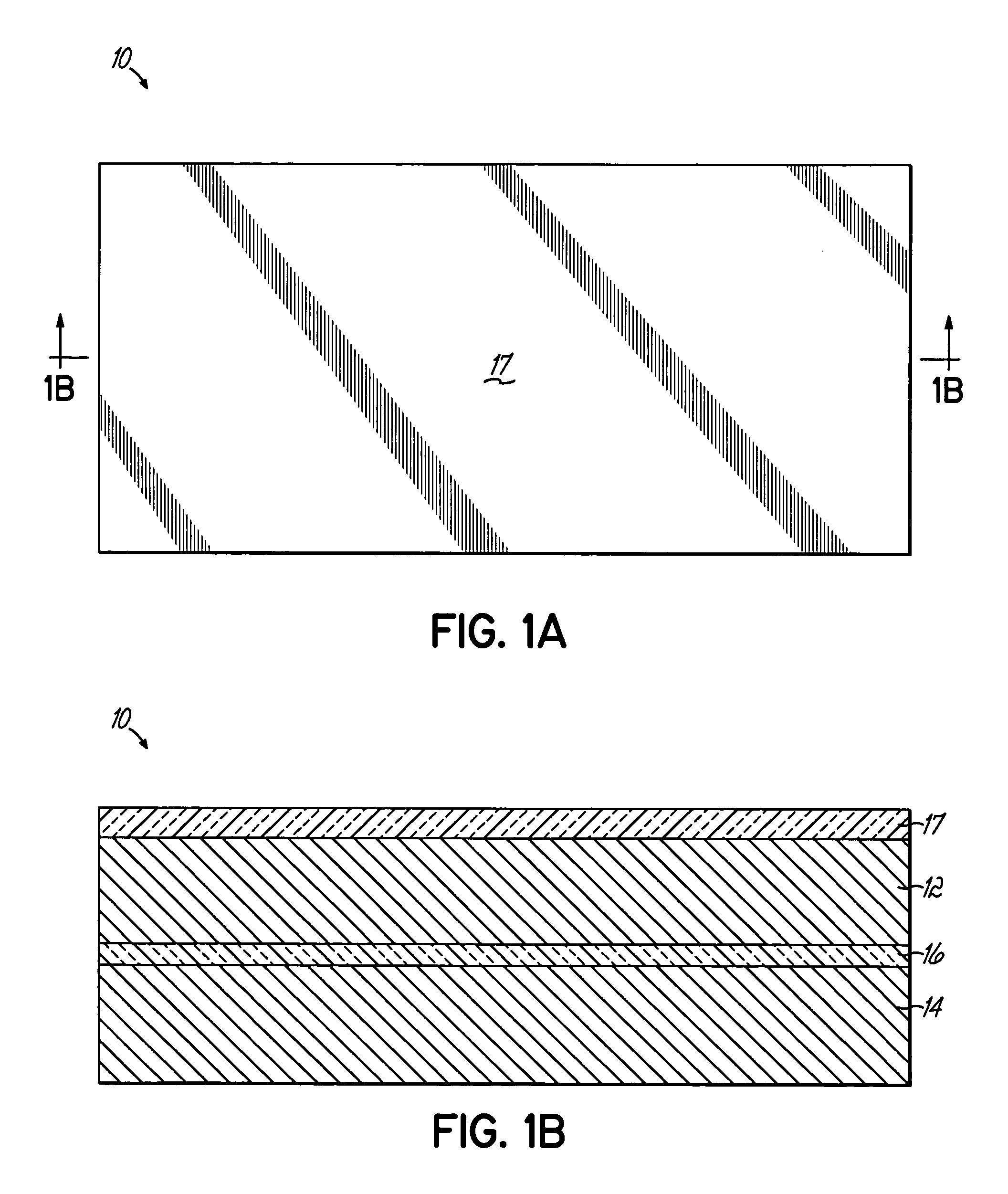
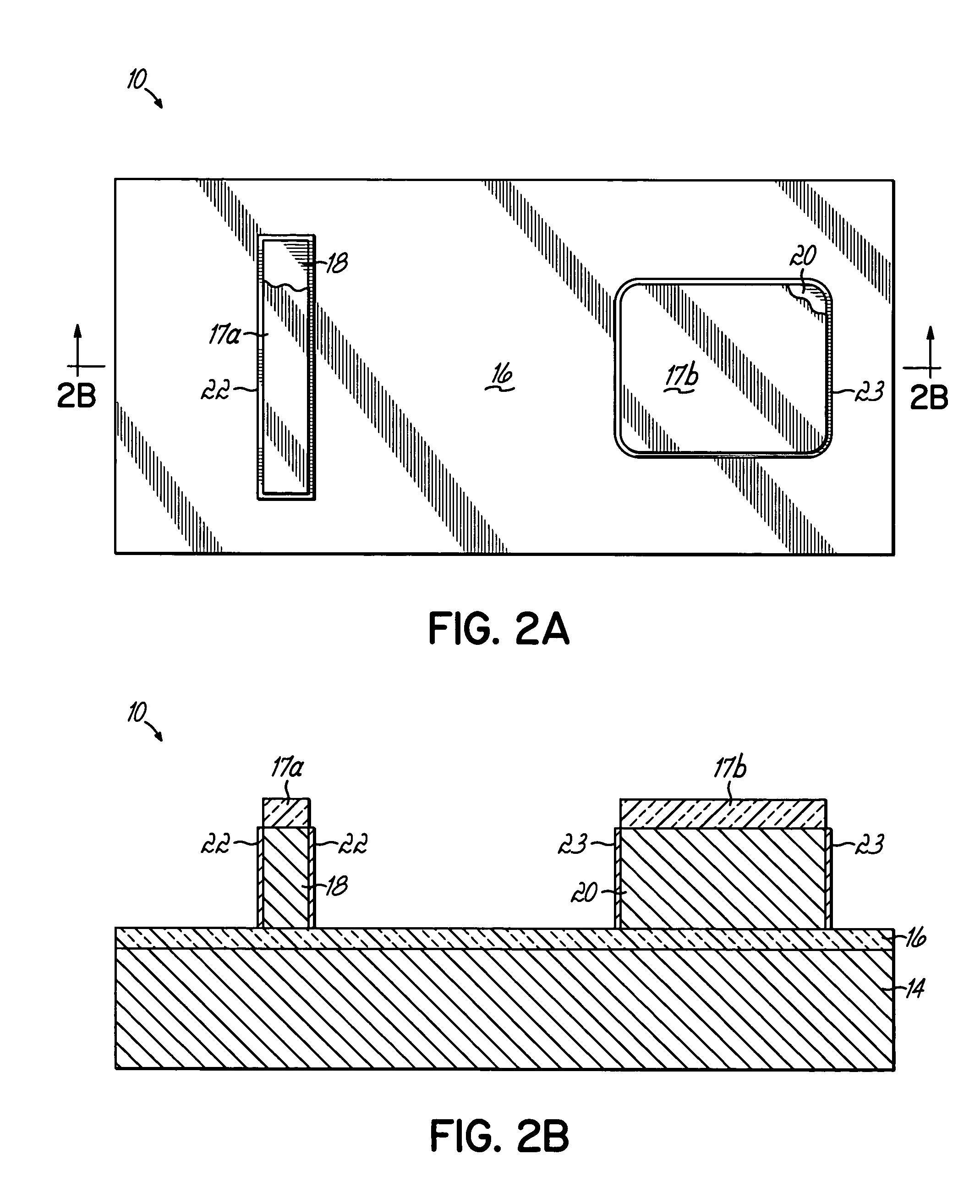
[0013]With reference to FIGS. 1A and 1B, a semiconductor-on-insulator (SOI) substrate, generally indicated by reference numeral 10, includes an active layer 12 of silicon, or another suitable semiconductor material, separated vertically from a handle wafer 14 by an insulating layer 16 (e.g., a buried oxide). Insulating layer 16 electrically isolates the active layer 12 from the handle wafer 14, which is typically silicon. The SOI substrate 10 may be fabricated by any standard technique, such as wafer bonding or a separation by implantation of oxygen (SIMOX) technique. In the illustrated embodiment of the invention, the silicon constituting the active layer 12 may be doped initially with an n-type dopant to render it n-type or a p-type dopant to render it p-type. The handle wafer 14 may be formed from any suitable semiconductor material including, but not limited to, silicon and polycrystalline silicon (polysilicon). The dielectric material constituting insulating layer 16 is typical...
PUM
 Abstract
Description
Claims
Application Information