
Method and apparatus for reducing power requirements in a multi gigabit parallel to serial converter

a serial converter and multi-gigabit technology, applied in the direction of generating/distributing signals, synchronising signal speed/phase control, multiplex communication, etc., can solve the problems of high clock-rate, complex requirements for data transmission between such devices and on individual ones of such devices, and the complexity of large-scale integration devices in digital logic design and implementation. , to achieve the effect of reducing the overall power requirements of a piso converter and high clock-ra

Inactive Publication Date: 2005-12-20
GULA CONSULTING LLC
View PDF10 Cites 9 Cited by
  • Summary
  • Abstract
  • Description
  • Claims
  • Application Information

AI Technical Summary

Benefits of technology

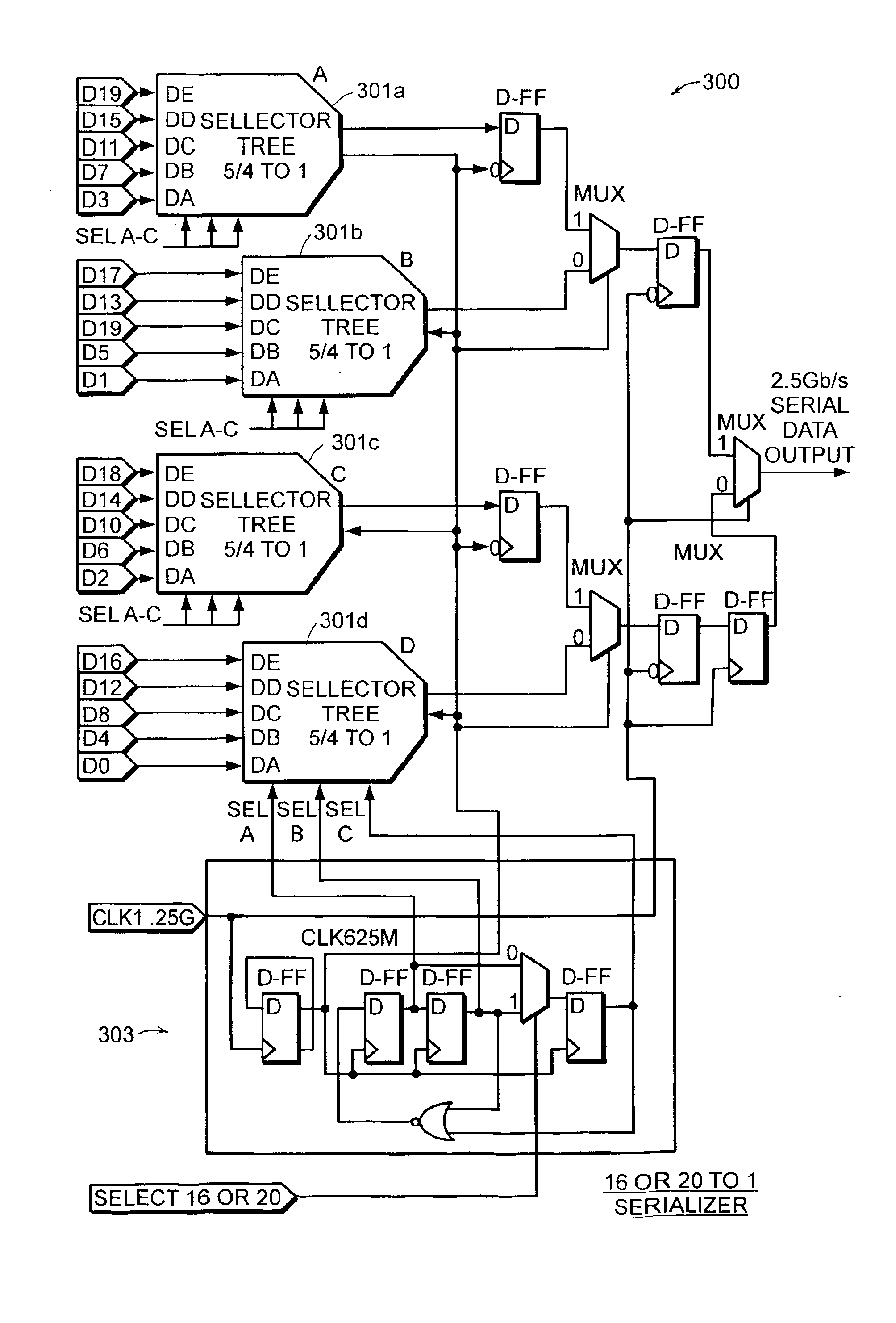
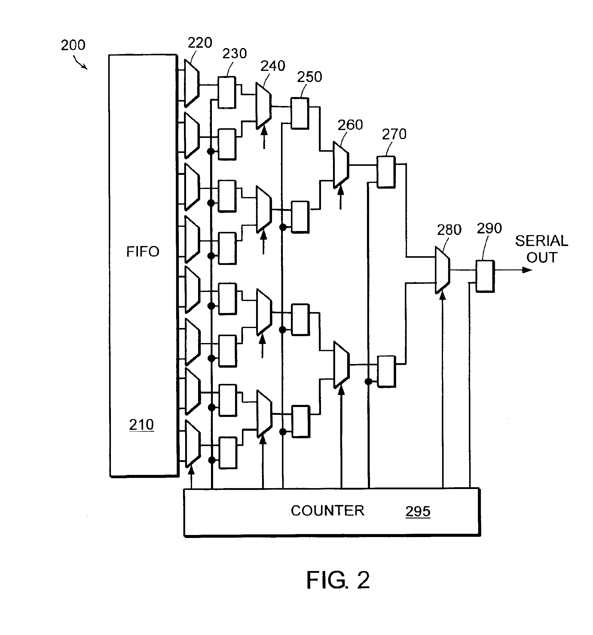
The present invention provides a variable-mode digital logic circuit for accepting a parallel data word and serializing it for output over a single one-bit wide trace. The circuit includes a plurality of parallel data traces, select-capable multiplexor circuits, and a ring counter for controlling the frequency of specific operations. The circuit can operate at different frequencies based on the number of select-capable multiplexor circuits. The invention also provides a method for reducing power requirements of a parallel-in-serial-out converter while maintaining a high clock-rate for gating out serial data from a parallel data source.

Problems solved by technology

The art of designing and implementing Large Scale Integration (LSI) devices and very large scale integration (VLSI) devices in digital logic has become more complex and sophisticated in recent years.
As semiconductor devices have become more complex in terms of circuitry and design, with shrinking device geometry, requirements for data transmission between such devices and on individual ones of such devices has also become more complex and demanding to maintain in operation.
Another problem with current technology is that analog circuitry is typically required in the sending and receiving IC devices to accommodate serial data transfer between the IC devices.
Analog circuitry is notoriously more difficult to implement than digital circuitry, and makers of digital IC devices are not anxious to suffer the yield losses attendant on adding analog circuitry to their devices.
Still, even with the known and perceived disadvantages of serial data transmission, the high cost and complexity of parallel data transmission systems is an increasing problem.
The high number of traces necessary on a PC board (for example) makes such support systems enormously complex and expensive to design and manufacture.
The higher and higher pin count makes such devices more complex to build and increases losses (lower yield) in fabrication.
One challenge in implementing parallel-in-to-serial-out (PISO) converters is that, in order to maintain the desired clock speed of the serial portion of the transmission, the entire converter is typically clocked at the same high speed.
This means that considerable power is consumed and cross contamination Oitter) between the traces is more likely to occur at higher levels.
The problem increases in chips that process larger bit-size words.

Method used


Image

  • Method and apparatus for reducing power requirements in a multi gigabit parallel to serial converter
  • Method and apparatus for reducing power requirements in a multi gigabit parallel to serial converter
  • Method and apparatus for reducing power requirements in a multi gigabit parallel to serial converter

Examples


Embodiment Construction

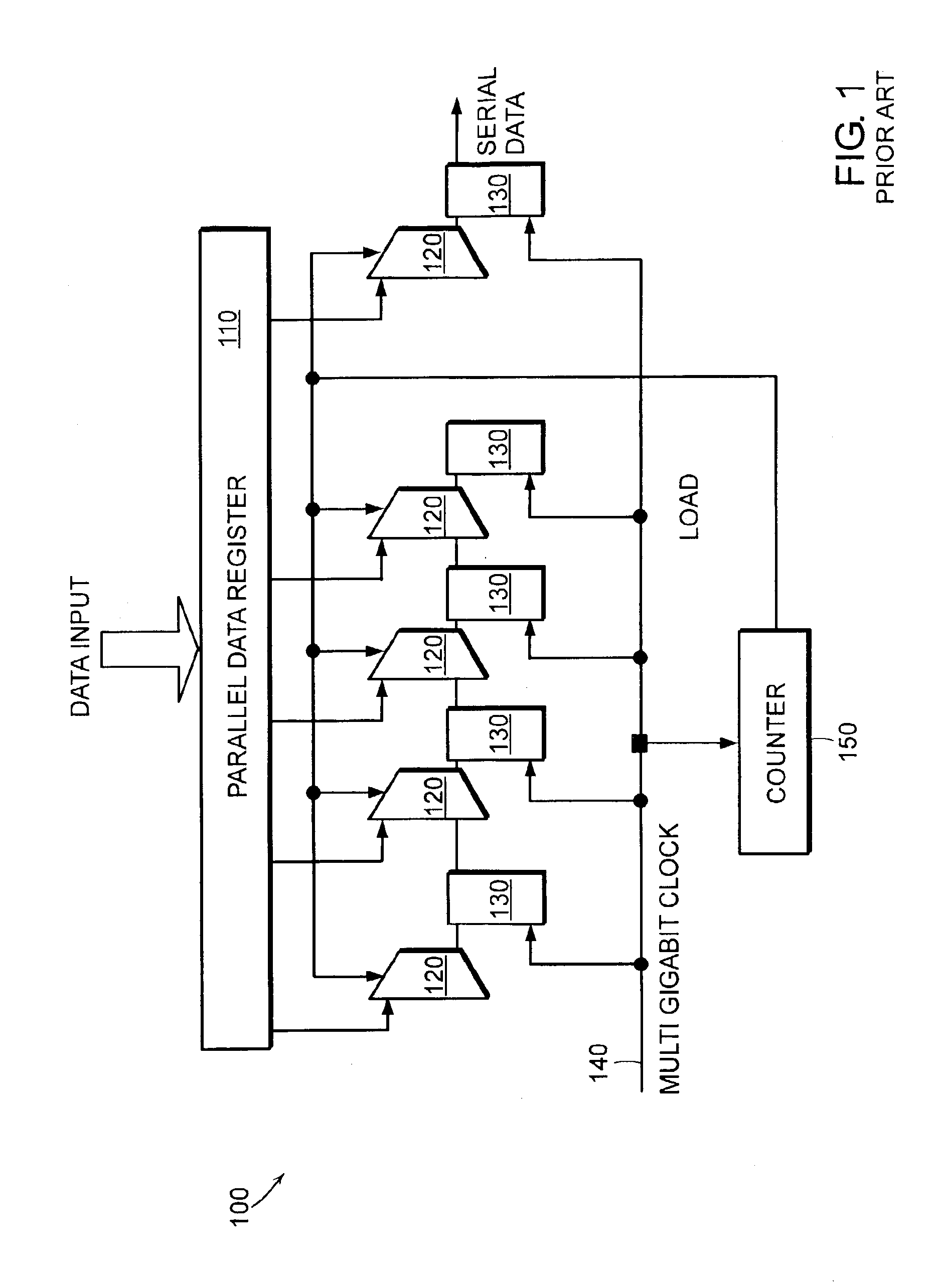
[0025]FIG. 1 is a circuit diagram illustrating a basic Parallel-in-to-Serial-Out (PISO) converter 100 according to prior art. In this prior art example, digital data input is loaded into a Parallel Data Register 110 represented in this diagram by a rectangular block labeled so. Actual data input is illustrated herein by a block arrow labeled “Data Input” proceeding into the Parallel Data Register. Output from the Parallel Data register is illustrated by a plurality of exit arrows or traces extending in parallel from the register 110. Though only 5 traces are illustrated in this example of PISO 100, the number of traces will depend on the size of the input word being processed. For example, in a 16-bit process there are 16 such traces, each trace carrying one bit.

[0026]A plurality of multiplexor (mux) circuits 120 are illustrated beneath Parallel Data Register 110 as is known in the art. Each mux circuit is dedicated to a single data path emanating from the register. Therefore, 5 mux...


PUM


Abstract

A variable-mode digital logic circuit is provided for accepting and serializing a parallel data word, so that the parallel data word may be transmitted from the digital logic circuit over a single one-bit wide trace. In some embodiments, the variable-mode digital logic circuit may include a plurality of parallel data traces for receiving the parallel dataword, a plurality of select-capable multiplexor circuits for sequentially activating certain ones of the parallel data traces and for multiplexing the received data into a serial data stream, a ring counter for controlling a frequency of specific operations performed within the circuit, and at least one additional multiplexor circuit array for receiving data output from the plurality of select-capable multiplexor circuits and for further serializing the received data for output on the single one-bit wide trace. The digital logic circuit may be adapted to operate according to one of a plurality of variable modes.

Description

CROSS-REFERENCE TO RELATED DOCUMENTS[0001]The present application is a continuation-in-part (CIP) of application Ser. No. 09 / 376,148 filed Aug. 17, 1999, now U.S. Pat. No. 6,233,294. The instant invention was disclosed in Disclosure Document #487034 filed on Jan. 10, 2001 in the USPTO.FIELD OF THE INVENTION[0002]The present invention is in the field of parallel to serial data transmission as it applies to computerized semiconductor devices and pertains more particularly to methods and apparatus for reducing power requirements in a multi-gigabit parallel to serial converter circuit.BACKGROUND OF THE INVENTION[0003]The art of designing and implementing Large Scale Integration (LSI) devices and very large scale integration (VLSI) devices in digital logic has become more complex and sophisticated in recent years. Sophisticated software design tools and automated techniques have replaced prior pencil and paper engineering practices once used to design semiconductor devices. As semiconduc...

Claims


Application Information

Patent Timeline
Patent Type & Authority Patents(United States)
IPC IPC(8): G06F1/10H04L7/02
CPCG06F1/10H04L7/02
Inventor MEASOR, GRAHAME CHRISTOPHER
Owner GULA CONSULTING LLC
Learn More