Bus system, memory system, printed circuit board and directional coupler

a bus system and memory technology, applied in the field of signal transmission, can solve the problems of reducing transmission efficiency, reducing the density of memory mounting, and the inability to make each interval less than a certain length, so as to achieve high density mounting, shorten the pitch of modules, and sharpen the waveform

Inactive Publication Date: 2005-12-20
LONGITUDE SEMICON S A R L
View PDF23 Cites 45 Cited by
  • Summary
  • Abstract
  • Description
  • Claims
  • Application Information

AI Technical Summary

Benefits of technology

[0012]As a means for solving the first problem, a line (main line) from a memory controller is folded, and directional couplers are formed both with respect to a line part before the fold and with respect to a line part after the fold. As a result, pitch of modules can be shortened, while wiring length of each coupler is maintained, and high-density mounting can be realized.
[0013]As a means for solving the second problem, a directional coupler that can generate forward crosstalk is formed in a T-shape. As a result, the backward crosstalk component and the forward crosstalk component are superposed into an NRZ signal in a transition time. By this operation, waveform can be sharpened, and dulling of w...

Problems solved by technology

However, shorter line length becomes a cause of reducing the transmission efficiency, i.e., degree of coupling, and thus, it is impossible to make each interval less than certain length.
Thus, a first problem is to realize high-density mounting of memories by making intervals between memory modules smaller.
A second problem is that, as transmission speed becomes higher in high-speed data transmission, waveform distortion increases owing to frequency-dependent effects such as the skin effect.
This appears as a phenomenon that pulse waveform becomes dull at its rising and falling shoulders, and owing to this influ...

Method used


Image

  • Bus system, memory system, printed circuit board and directional coupler
  • Bus system, memory system, printed circuit board and directional coupler
  • Bus system, memory system, printed circuit board and directional coupler

Examples


first embodiment

[0045]A first embodiment will be described referring to FIG. 1.

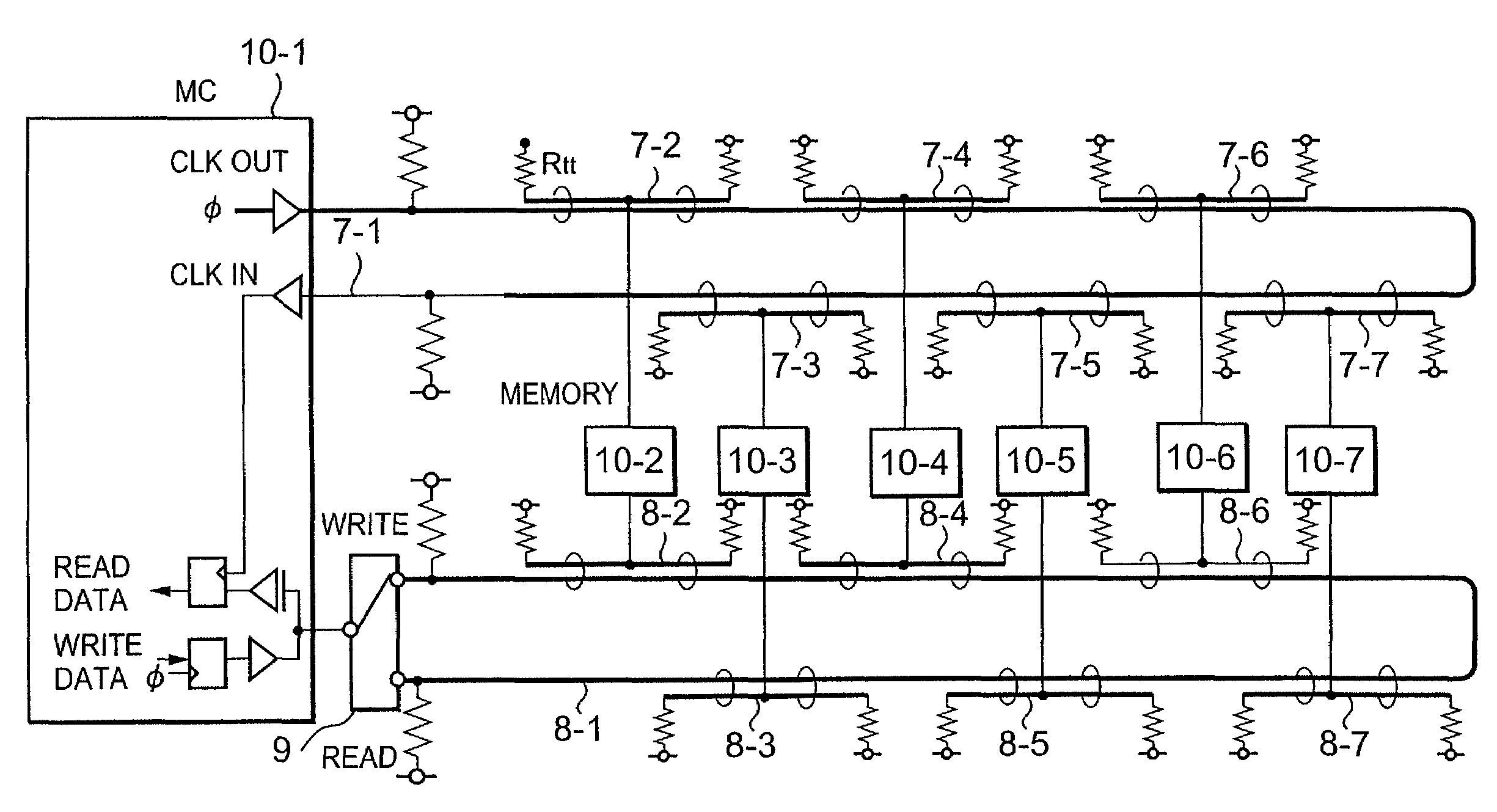
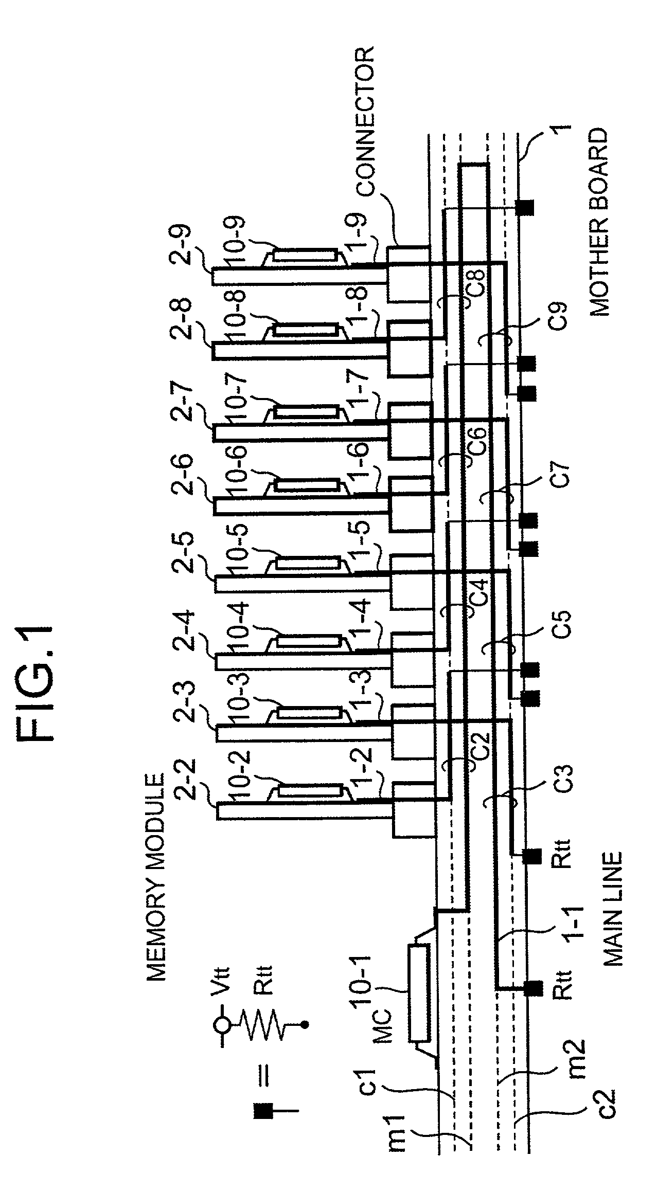
[0046]A reference numeral 10-1 refers to an LSI chip (hereinafter referred to as MC: Memory Controller) having a control function as a memory controller, and 2-2–2-9 to memory modules each mounted with a plurality of memory chips 10-2–10-9. A printed circuit board 1 is a mother board that is mounted with MC 10-1 and the memory modules 2-2–2-9 and has lines permitting data transfer between MC 10-1 and the memory chips 10-2–10-9 within the memory modules 2-2–2-9. The memory modules 2-2–2-9 are connected to the mother board via connectors.

[0047]MC 10-1 carries out operations of data read and write into the memory chips 10-2–10-9. Reference numerals 1-1–1-9 refer to lines for data transfer carried out for those read and write operations. Among these lines, the line 1-1 connected to MC 10-1 is particularly called a main line.

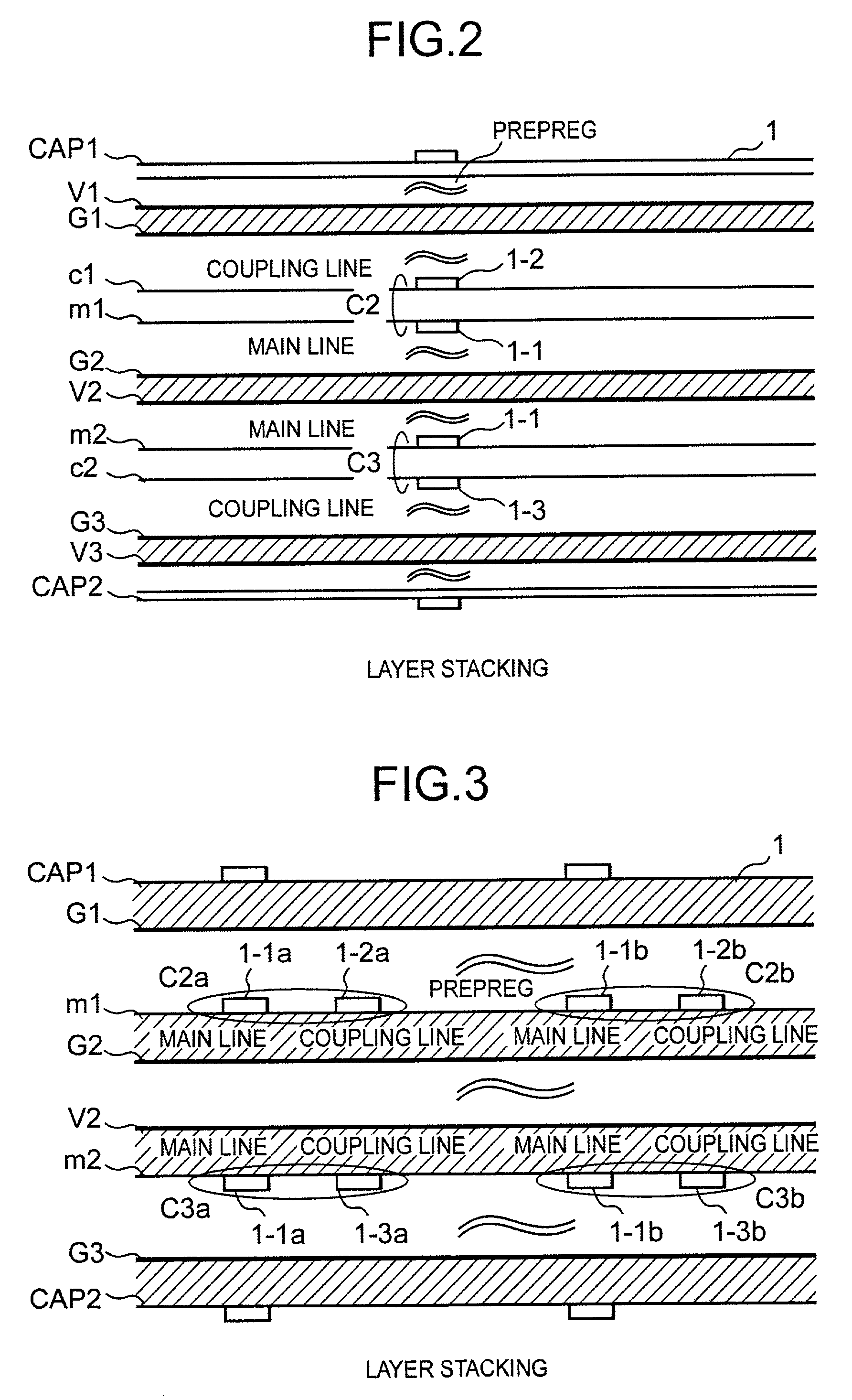
[0048]Broken lines m1, c1, m2 and c2 within the mother board refer to signal layers within the board, ...

second embodiment

[0063]A second embodiment is shown in FIG. 6. Also, arrangement and wiring in FIG. 6 can realize high-density mounting of memory modules. In FIG. 6, like symbols have like functions as in FIG. 1. FIG. 6 differs from FIG. 1 in construction of directional couplers. Namely, a main line 1-1 is arranged straight, and the directional couplers are located on both the left and right sides of the main line in an alternating way, with the other set of lines 1-2–1-6 of the directional couplers C2–C6 being on the other side.

[0064]FIG. 7 shows an example of wiring of the mother board 1 of this FIG. 6. FIG. 7 is a view of the memory system of FIG. 6 seen from the side of the upper surface. The lines shown in FIG. 7 correspond to one bit of data, among the many lines existing in the same signal layer. In the mother board 1, there are arranged MC 10-1 and connectors 2-6 to which the memory modules 2-2–2-6 are to be connected. Data signal in the memory system is connected through a bus, so that one ...

third embodiment

[0069]A third embodiment is shown in FIG. 8. By folding a main line in a same layer as shown in FIG. 8, high-density mounting of memory modules can be realized.

[0070]FIG. 8 has the same structure as FIG. 1 from the electric viewpoint. Similarly to FIG. 7, FIG. 8 is a view of a mother board 1 seen from the side of its upper surface. In FIG. 8, the main line 1-1 from MC 10-1 is folded in a same signal layer within the board (mother board) 1. A signal from MC 10-1 is coupled to signal pins located in the same position in connectors 2-6. The main line 1-1 is wired in the same layer, to enclose those signal pins.

[0071]With respect to this main line 1-1, lines 1-2–1-6 from the connectors 2-6 are formed such that couplers C2–C6 correspond to every other connectors arranged successively, being coupled to the main line 1-1 before folding and the main line 1-1 after folding. Of course, the connectors 2-6 and the main line 1-1 are terminated, and there is no reflection distortion at their term...


PUM


Abstract

A bus system for carrying out data transfer between one bus master and a plurality of bus slaves. The bus system includes plural directional couplers which are formed by arranging respective parts of lines drawn from the bus slaves, without being in contact with, in the neighborhood of, and in parallel with a line drawn from the bus master. The line drawn from the bus master to a terminating resistance is wired to be folded. The directional couplers are further formed by arranging parts of the lines drawn from the bus slaves alternatively with respect to a first line part of the line drawn from the bus master ranging from the bus master to a fold of the line drawn from the bus master and with respect to a second line part of the line drawn from the bus master ranging from the fold to the terminating resistance.

Description

BACKGROUND OF THE INVENTION[0001]1. Field of the Invention[0002]The present invention relates to a technique of signal transmission between devices such as multiple processors and memories (for example, between digital circuits constructed by CMOSs or between their functional blocks) in an information processing apparatus, and in particular to a technique for speeding up bus transmission which a plurality of elements are connected to a same transmission line for transferring data. In particular, the present invention relates to a bus to which a plurality of memory modules and a memory controller are connected and to a system using that bus.[0003]2. Description of Related Art[0004]As a bus system that is connected with many nodes and intended for high-speed data transfer, is mentioned a non-contact bus line of Japanese Unexamined Patent Laid-Open No. 7-141079 (U.S. Pat. No. 5,638,402). FIG. 5 shows the basic system of the conventional technique. In this technique, data transfer betwe...

Claims


Application Information

Patent Timeline
IPC IPC(8): G06F3/00G06F1/00G06F12/00G06F13/16H01P5/00H01P5/18H05K1/00H05K1/02H05K1/14
CPCH05K1/0228H05K1/0246H05K1/0298H05K1/14H05K2201/044H05K2201/09236H05K2201/09627H05K2201/10022
Inventor OSAKA, HIDEKITSUNEHIRO, TAKASHIKIMURA, KOICHIHATANO, SUSUMUITO, KAZUYASUGANO, TOSHIOKOMATSU, TOYOHIKO
Owner LONGITUDE SEMICON S A R L
Why Eureka
Try Eureka