Reflection-transmission type liquid crystal display device and method for manufacturing the same

a liquid crystal display and reflection-transmission technology, applied in semiconductor devices, instruments, optics, etc., can solve the problems of metal corrosion during the subsequent cog bonding process, complicated process, and complicated manufacturing process, so as to prevent galvanic corrosion, simplify manufacturing process, and improve manufacturing efficiency

Inactive Publication Date: 2005-12-27
SAMSUNG DISPLAY CO LTD
View PDF9 Cites 31 Cited by
  • Summary
  • Abstract
  • Description
  • Claims
  • Application Information

AI Technical Summary

Benefits of technology

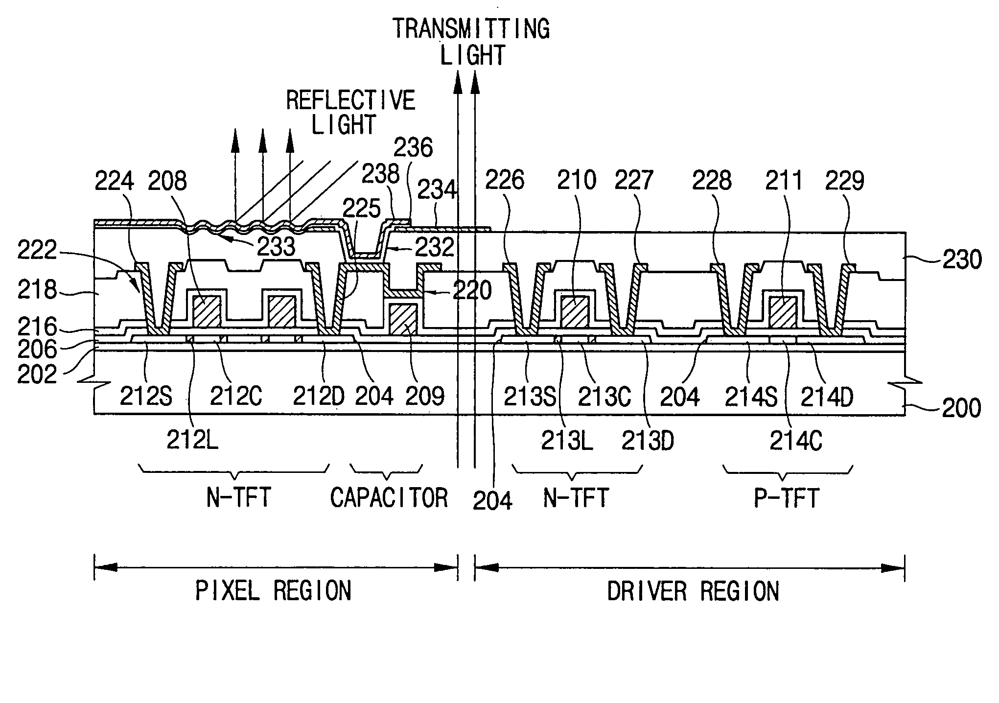
[0045]According to the present invention, a multilayered pixel electrode of the liquid crystal display device has a structure in which the transparent electrode is formed as the lower layer and the transparent electrode is in direct contact with the reflective layer. Preferably, in order to prevent the galvanic corrosion from being generated between the transparent electrode and the reflective electrode, the barrier metal layer pattern having the etching rate identical to that of the reflective electrode is interposed between the transparent electrode and the reflective electrode. Therefore, the manufacturing process can be simplified by reducing at least one mask in comparison with the conventional method in which the buffer layer is formed between the transparent electrode and the reflective electrode. Also, the manufacturing process can be more simplified because the pixel electrode is formed using one mask when the half-tone mask or the slit mask is utilized.
[0046]In addition, after depositing the reflective layer, the annealing of the reflective layer is performed at a temperature of about 200° C. for about 1 to about 2 hours to thereby prevent the lifting of the reflective electrode in the pixel electrode having the transparent electrode as the bottom layer.
[0047]Furthermore, the pad electrodes are formed of the same layer as the transparent electrode composed of a conductive oxide layer, so that the pad reliability can increase without the metal corrosion during COG bonding process.

Problems solved by technology

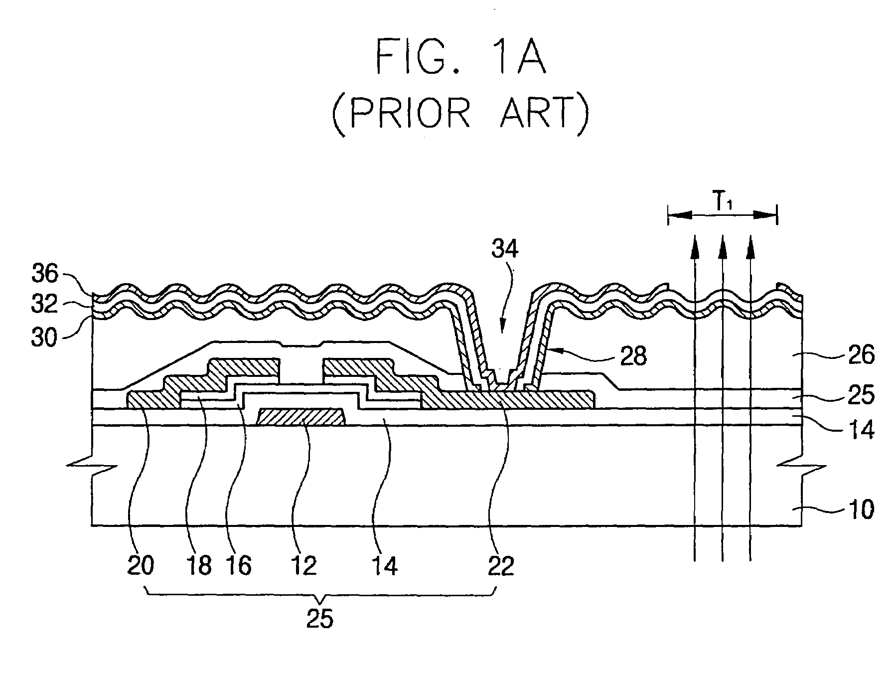
Hence, the manufacturing process is more complicated because an additional photolithography process is needed for etching the insulating layer to form the contact hole connecting the reflective electrode 36 to the thin film transistor.
However, such process is complicated since at least one mask is required for patterning the buffer layer.
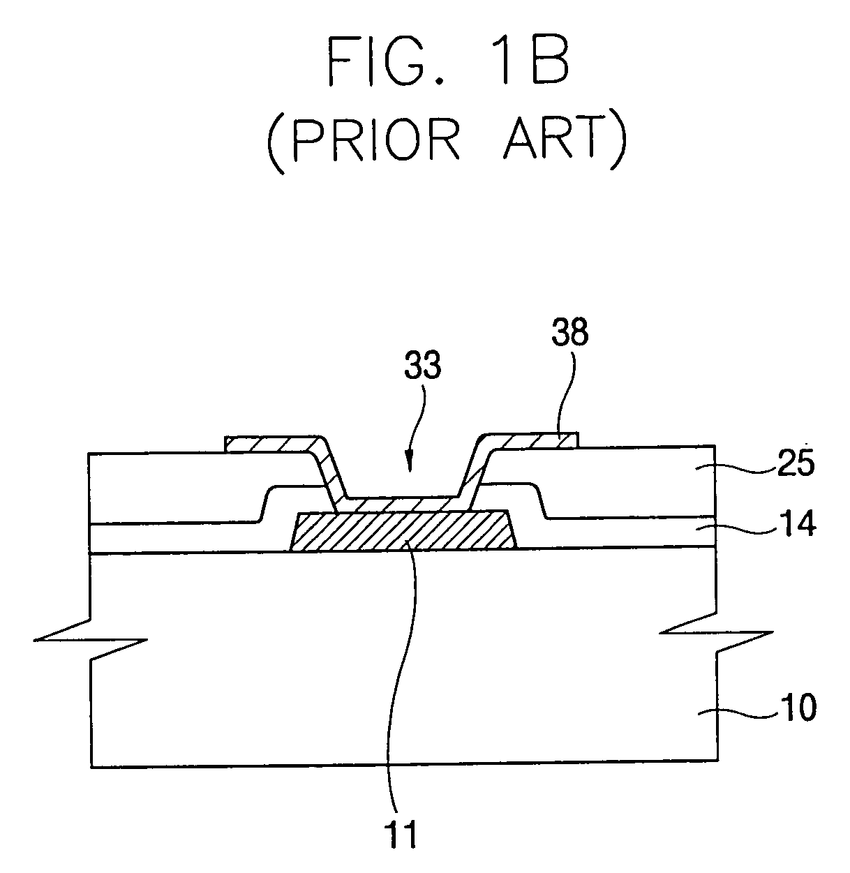
Furthermore, metals are corroded during subsequent COG bonding process since the pad electrodes and the reflective electrode are formed from the same layer.

Method used


Image

  • Reflection-transmission type liquid crystal display device and method for manufacturing the same
  • Reflection-transmission type liquid crystal display device and method for manufacturing the same
  • Reflection-transmission type liquid crystal display device and method for manufacturing the same

Examples


embodiment 1

[0060]FIGS. 3A to 3C are cross-sectional views showing a reflection-transmission type liquid crystal display device according to a first embodiment of the present invention. The liquid crystal display device in FIGS. 3A to 3C includes an amorphous silicon type thin film transistor having a bottom-gate structure. FIG. 3A illustrates a display region where the thin film transistor is formed. FIGS. 3B and 3C show a gate pad region and a data pad region, respectively.

[0061]Referring to FIGS. 3A to 3C, a gate wiring composed of a first metal layer such as chrome (Cr) or aluminum-neodymium (Al—Nd) is formed on an insulation substrate 100 made of glass, quartz, or sapphire. The gate wiring includes a gate line (not shown) extended in a first direction, a gate electrode 102 of a thin film transistor 150 branched from the gate line, and a gate pad 104 connected to the end of the gate line for applying a scanning voltage to the gate electrode 102.

[0062]A gate insulation layer 106 is formed on...

embodiment 2

[0094]FIG. 11 is a cross-sectional view showing a reflection-transmission type liquid crystal display device according to a second embodiment of the present invention.

[0095]Referring to FIG. 11, the reflection-transmission type liquid crystal display device according to the second embodiment is the same as that of the first embodiment except one thing. The difference between the second embodiment and the first embodiment is that the transparent electrode 124 is formed on the passivation layer 120 excluding the first contact hole 122, and the barrier metal layer pattern 128 and the reflective electrode 130 are formed on the first contact hole 122 and the transparent electrode 124 so as to be in direct contact with the drain electrode 114 of the thin film transistor 150 through the first contact hole 122.

[0096]In case that the data wiring including the drain electrode 114 is formed of a metal film including a chrome (Cr), a thin chrome oxide film is grown on the surface of the metal f...

embodiment 3

[0098]FIG. 12 is a cross-sectional view showing a reflection-transmission type liquid crystal display device according to a third embodiment of the present invention.

[0099]Referring to FIG. 12, the reflection-transmission type liquid crystal display device according to the third embodiment is the same as that of the first embodiment except one thing. The difference between the third embodiment and the first embodiment is that the barrier metal layer pattern 128 and the reflective electrode 130 are formed only on the transparent electrode 124 excluding the first contact hole 122.

[0100]At this time, since the reflective electrode 130 is electrically connected to the transparent electrode 124 via the barrier metal layer pattern 128, a signal is normally transmitted to the pixel electrode from the thin film transistor.


PUM

PropertyMeasurementUnit
temperatureaaaaaaaaaa

Abstract

Disclosed are a liquid crystal display (LCD) device and a method for manufacturing the LCD device. The LCD device has a substrate including a display region and a pad region located in a periphery of the display region, the display region having a transparent electrode, the pad region having a pad electrode. The transparent electrode and the pad electrode are formed from the same layer. A reflective electrode having a transmission window exposing a portion of the transparent electrode is formed on the transparent electrode. The manufacturing process can be simplified because the transparent electrode is directly connected to the reflective electrode. Since the pad electrode is formed of the same layer as the transparent electrode, no metal corrosion occurs to thereby increase the pad reliability during COG bonding.

Description

[0001]This application is a divisional of U.S. application Ser. No. 10 / 218,549, filed on Aug. 14, 2002.BACKGROUND OF THE INVENTION[0002]1. Field of the Invention[0003]The present invention relates to a reflection-transmission type liquid crystal display device and a method for manufacturing the same, and more particularly to a reflection-transmission type liquid crystal display device and a method for manufacturing the same in which a pad electrode is formed with the same layer as in a transparent electrode to enhance the pad reliability.[0004]2. Description of the Related Art[0005]Among flat panel devices, liquid crystal display (LCD) devices have been widely utilized for various electronic devices because the LCD devices are light, thin, have low power dissipation, and are capable of displaying a high quality image.[0006]LCD devices generally comprise transmission, reflection, and reflection-transmission types. The transmission type LCD device displays information by using a light...

Claims


Application Information

Patent Timeline
Patent Type & Authority Patents(United States)
IPC IPC(8): G02F1/1368G02F1/1335G02F1/1343G02F1/1345G02F1/1362H01L21/336H01L29/786
CPCG02F1/133555G02F1/1345G02F1/13454G02F1/13458G02F1/136213G02F1/136227G02F2001/133388G02F2001/136236G02F2001/13685H01L27/1248G02F1/133388G02F1/136236G02F1/13685G02F1/1335
Inventor YOU, CHUN-GI
Owner SAMSUNG DISPLAY CO LTD
Why Eureka
Try Eureka