Semiconductor package with heat dissipating structure

a technology of semiconductors and heat dissipation structures, applied in the direction of electrical apparatus construction details, basic electric elements, lighting and heating apparatus, etc., can solve the problems of heat dissipation, performance of multi-chip packages, and improve the structure of fcbga packages, so as to improve the adhesion of the second heat sink, and improve the heat dissipation

Active Publication Date: 2005-12-27
SILICONWARE PRECISION IND CO LTD
View PDF11 Cites 24 Cited by
  • Summary
  • Abstract
  • Description
  • Claims
  • Application Information

AI Technical Summary

Benefits of technology

[0014]An object of the present invention is to provide a semiconductor package having a heat dissipating structure, which is formed with low cost without the need of forging.
[0015]Another object of the invention is to provide a semiconductor package having a heat dissipating structure, which has reduced package height.

Problems solved by technology

Since a multi-chip package generates more heat than a single-chip package, heat dissipation is a crucial factor affecting the performance of the multi-chip package.
As a result, the configuration of the above upwardly-recessed shaped heat sink sets a limitation in improving the FCBGA package structure and is not desirable for realization of packages with high heat dissipating efficiency, low fabrication cost and small size.
This method is limited by operation of the forging machine and forging hammer and its equipment cost.
This is not favorable to the throughput and would cause an increase in the production cost when the size of the heat sink is changed.
Furthermore, the forging method has a problem of limited molding precision.
As a result, the overall size of the package is difficult to be reduced, which is not favorable to the current trend of size miniaturization.
The heat sink formed by forging is limited to the type and size of the forging hammer, thereby not allowing desirable flexibility in size and shape of the heat sink for increasing its heat dissipating area.
Due to design limitations, the fins 67 are located only right above the flat part 60a, which results in significant increase in the total thickness of the package.
However, with the limitation of the size of the forging hammer, the size and shape of the heat sink 60 cannot be flexibly modified according to the layout on the substrate 62, such that fabrication of a batch of new products is required, thereby setting a substantial limitation to wire routing.
When the process is completed, a residual stress is left at a periphery of the accommodating space of the heat sink due to stress concentration, which damages the crystal cells of the copper or aluminum.
Since the periphery of the flat part is sustained by the supporting part, the thermal strain is difficult to release, and the deformation of the heat sink as shown in FIG. 23 is generated.
Slight modification to the structure of the heat sink formed by the current forging process cannot overcome all the problems in the art.

Method used


Image

  • Semiconductor package with heat dissipating structure
  • Semiconductor package with heat dissipating structure
  • Semiconductor package with heat dissipating structure

Examples


first preferred embodiment

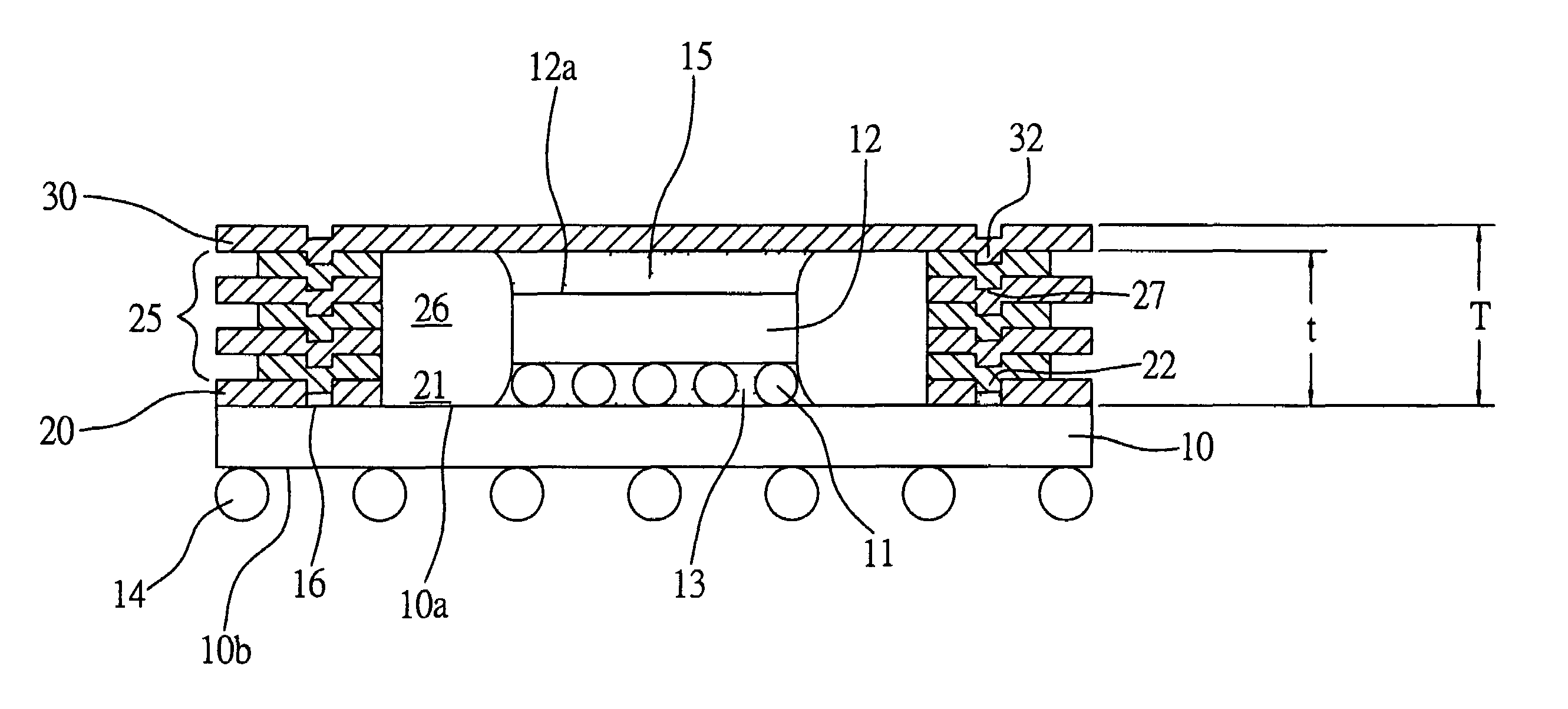
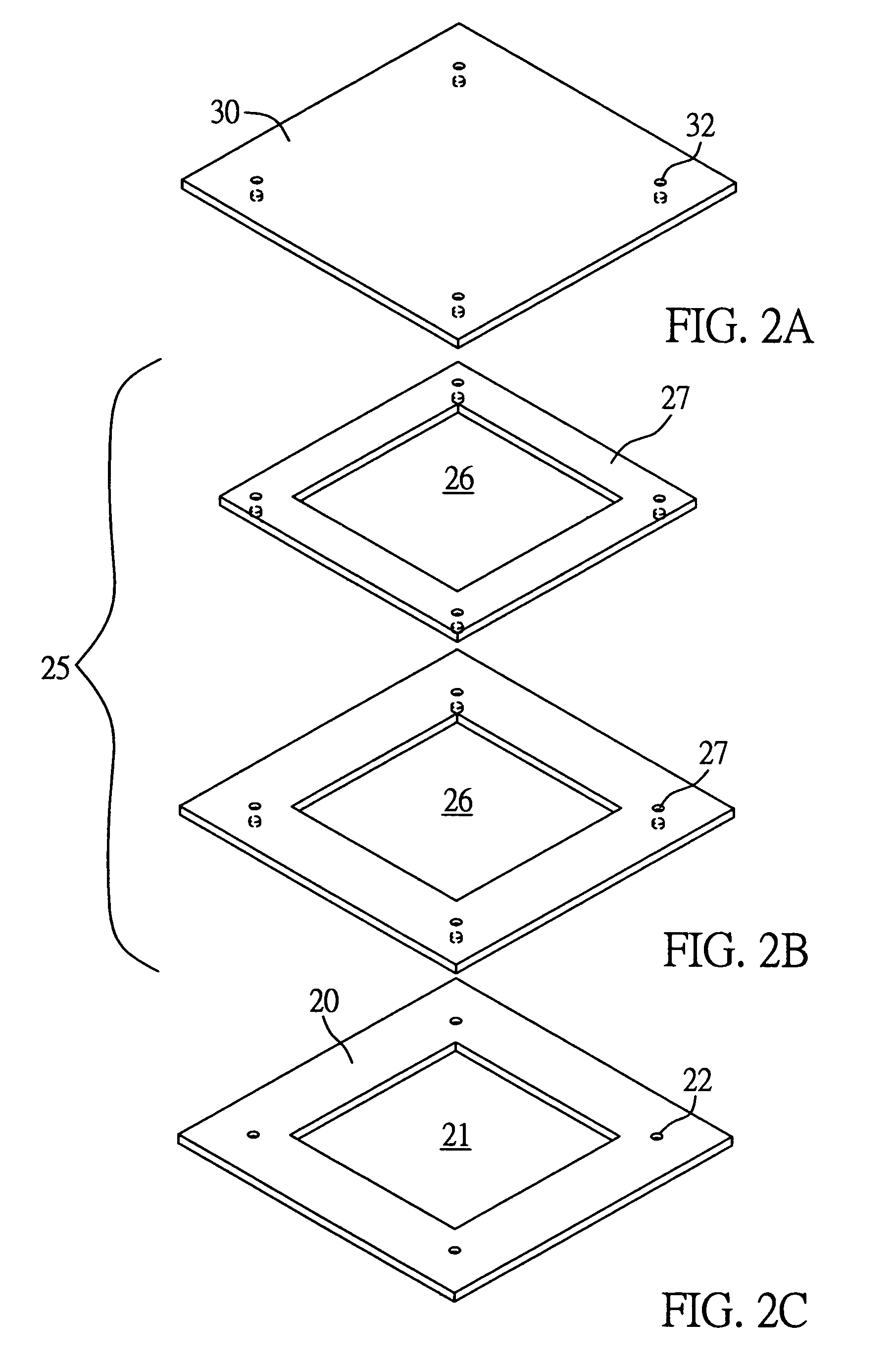
[0055]FIG. 1 is a cross-sectional view of a semiconductor package having a heat dissipating structure according to a first embodiment of the invention. The semiconductor package is a flip-chip ball grid array (FCBGA) and includes a substrate 10 as a chip carrier. A chip 12 is mounted on and electrically connected to a first surface 10a of the substrate 10 via bumps 11. An insulation material 13 fills gaps between the bumps 11 to form an underfill. A bottom heat sink 20 is mounted on the first surface 10a of the substrate 10. Interlayer heat sinks 25 are stacked on the bottom heat sink 20. A top heat sink 30 is stacked on the top of the interlayer heat sinks 25. Solder balls 14 are attached on a second surface 10b of the substrate 10 and electrically connected to the bumps 11. An adhesive 16 is applied over the first surface 10a of the substrate 10 for attaching the bottom heat sink 20 on the substrate 10. The top heat sink 30 is attached on a non-active surface of the chip 12 via a ...

second preferred embodiment

[0061]Although the invention is illustrated with the description of the above embodiment, equivalents thereof may be also envisaged. FIG. 4 is a cross-sectional view of a stack of heat sinks according to a second embodiment of the invention. The stack of heat sinks of this second embodiment has the same elements as those of the first embodiment, except that the heat sinks are arranged differently from the first embodiment. In the first embodiment, the edge of the hollow portion 26 of each heat sink 25 is aligned with one another while the outer edges of the heat sinks 25 are arranged in a stagger manner to increase the heat dissipation area of the heat sinks 25. In this second embodiment, an outer edge 25c of each interlayer heat sink 25 is aligned with one another. The inner edges 25d of the interlayer heat sinks 25 (i.e. periphery of the first hollow portion 26) are arranged in a stagger manner so that the chip accommodating space defined by the inner edges of the beat sinks 25 is...

third preferred embodiment

[0062]This third embodiment combines the first and second embodiments, as shown in FIG. 5. Both inner and outer edges of each heat sink are not aligned with one another. Thereby, the heat dissipation area is further increased to provide higher heat dissipation performance.


PUM


Abstract

A semiconductor package with a heat dissipating structure includes a substrate, a chip and a heat dissipating structure. The chip is mounted on and electrically connected to the substrate. The heat dissipating structure includes a first heat sink having at least one positioning portion, and at least one second heat sink having at least one second positioning portion and at least one hollow portion. The second heat sink is mounted on the substrate, and the first positioning portion of the first heat sink is attached to the second positioning portion of the second heat sink, allowing the chip to be accommodated in a space defined by the first heat sink, the hollow portion of the second heat sink and the substrate. This semiconductor package has good heat dissipating efficiency and is cost-effective to fabricate.

Description

FIELD OF THE INVENTION[0001]The present invention relates to semiconductor packages with heat dissipating structures, and more particularly, to a semiconductor package with a heat dissipating structure achieved with lowered cost and reduced package thickness.BACKGROUND OF THE INVENTION[0002]A flip-chip ball grid array (FCBGA) semiconductor package incorporates a flip-chip structure and a ball grid array, wherein an active surface of a chip is electrically connected to a first surface of a substrate via a plurality of solder bumps, and a plurality of solder balls are mounted on a second surface of the substrate opposite to the first surface and serve as input / output (I / O) connections. This type of package structure has an advantage of great decrease in size, without using conventional bonding wires. Therefore, impedance or resistance of signal transmission can be reduced while electrical performance would be improved, making the FCBGA package become the mainstream of packaging techno...

Claims


Application Information

Patent Timeline
Patent Type & Authority Patents(United States)
IPC IPC(8): H01L21/48H01L21/56H01L23/055H01L23/10H01L23/367H01L23/467H01L25/065
CPCH01L21/4882H01L23/055H01L23/10H01L23/3675H01L23/467H01L21/563H01L23/3672H01L25/0655H01L2224/16145H01L2224/32145H01L2224/73204H01L2224/73207H01L2224/73253H01L2924/15311H01L2924/16152H01L2924/16195H01L2924/16315H01L2924/19105H01L2924/3011H01L2924/3511H01L2224/16225H01L2224/32225H01L2224/48227H01L2924/00
Inventor HUANG, CHIEN-PINGPU, HAN-PINGCHEN, CHIN-TELIN, CHANG-FU
Owner SILICONWARE PRECISION IND CO LTD
Why Eureka
Try Eureka