Ion recoil implantation and enhanced carrier mobility in CMOS device

a cmos device and recoil technology, applied in the field of ion recoil implantation and enhanced carrier mobility in cmos devices, can solve the problems of increasing the time and cost of fabrication required to form the ic, unable to meet the high performance requirements, and the technique of scaling either the gate dielectric or the channel length or both has been difficult and/or impractical to achieve high performance requirements, etc., to achieve enhanced carrier mobility, carrier mobility, and high carrier mobilities

Inactive Publication Date: 2006-01-03
BELL SEMICON LLC
View PDF24 Cites 9 Cited by
  • Summary
  • Abstract
  • Description
  • Claims
  • Application Information

AI Technical Summary

Benefits of technology

[0010]Strained Si and Ge alloys (e.g. the SiGe layer) are known to have higher carrier mobilities than the materials more commonly used in the channel regions of CMOS devices. Therefore, the carrier mobility is enhanced for the channel region of the CMOS devices in ICs incorporating the present invention. The carrier mobility enhancement is particularly beneficial in ICs having CMOS devices formed with sub-0.1 micron technology, because it is not necessary to aggressively scale the length of the channel regions or the gate dielectric of the CMOS devices. The carrier mobilities under the present invention may not be enhanced as much as those under the strained Si technique described in the background. However, the present invention involves simpler, less expensive and less time-consuming fabrication procedures, making the present invention an improvement over the prior technique.
[0012]The CMOS device is preferably, but not necessarily, formed using sub-0.1 micron technology. Additionally, according to various embodiments of the present invention, the CMOS device is preferably formed 1) on the Ge-containing region of the semiconductor substrate, 2) on a strained Si region within the semiconductor substrate formed above the Ge-containing region of the semiconductor substrate or 3) on a strained Si layer that is formed above the semiconductor substrate on the Ge-containing region of the semiconductor substrate. Thus, the channel region of the CMOS device preferably includes the strained Si region and / or the Ge-containing region. In each of these cases, therefore, the carrier mobility in the channel region of the CMOS device is preferably greater than that in the semiconductor substrate outside of either the Ge-containing region or the strained Si region. The enhanced carrier mobility is particularly significant for enabling the present invention to meet the performance requirements of sub-0.1 micron technology using the relatively simple Ge-recoil procedure, instead of the complex and costly techniques described in the background.

Problems solved by technology

As attempts have been made to scale down CMOS technology into the sub-0.1 micron dimensions, however, the performance requirements for the CMOS devices have proven so stringent that the technique of scaling either the gate dielectric or the channel length or both has been a very difficult and / or impractical solution for meeting the high performance requirements.
The epitaxial growth steps increase the time and cost of fabrication required to form the IC.
Thus, there is a tradeoff between the performance characteristics and the cost of the resulting IC.
Additionally, the presence of the strained Si layer 104 sets limitations on the temperatures at which any subsequent processing steps may be performed, thereby limiting the flexibility with which the subsequent processing steps may be performed.
Furthermore, the relatively thick SiGe film 100 acts as a thermal insulation layer, so the CMOS transistors formed thereon are susceptible to self-heating during operation of the IC, thereby degrading the performance capability of the IC.
Furthermore, this technique is prone to defects, which may occur in the SiGe film 100 and, thus, propagate into the strained Si layer 104 and higher layers of materials.
Such defects may involve threaded dislocations in the crystalline structure of the various layers that negatively impact carrier mobility, gate oxide quality and overall device performance.

Method used


Image

  • Ion recoil implantation and enhanced carrier mobility in CMOS device
  • Ion recoil implantation and enhanced carrier mobility in CMOS device
  • Ion recoil implantation and enhanced carrier mobility in CMOS device

Examples


Embodiment Construction

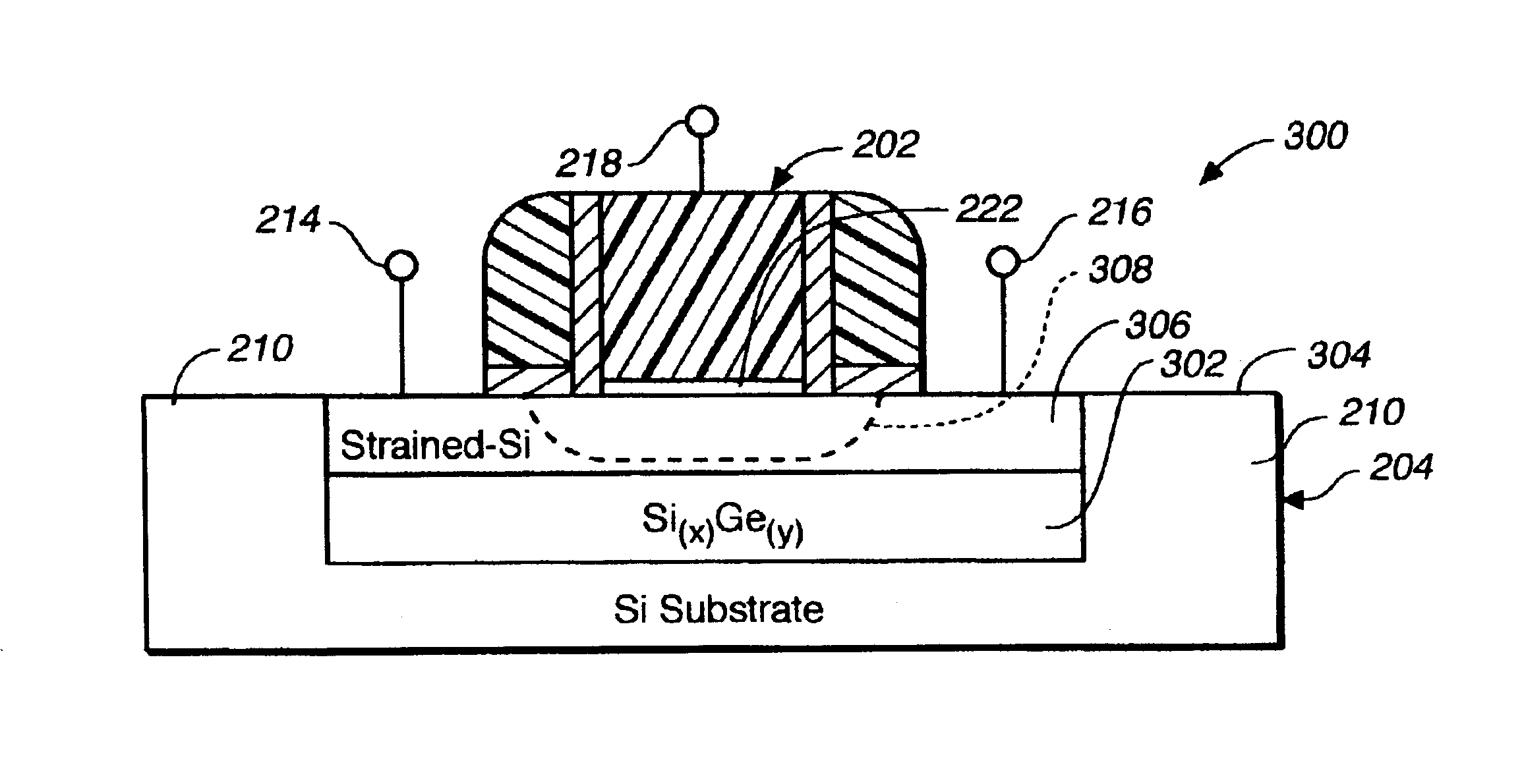
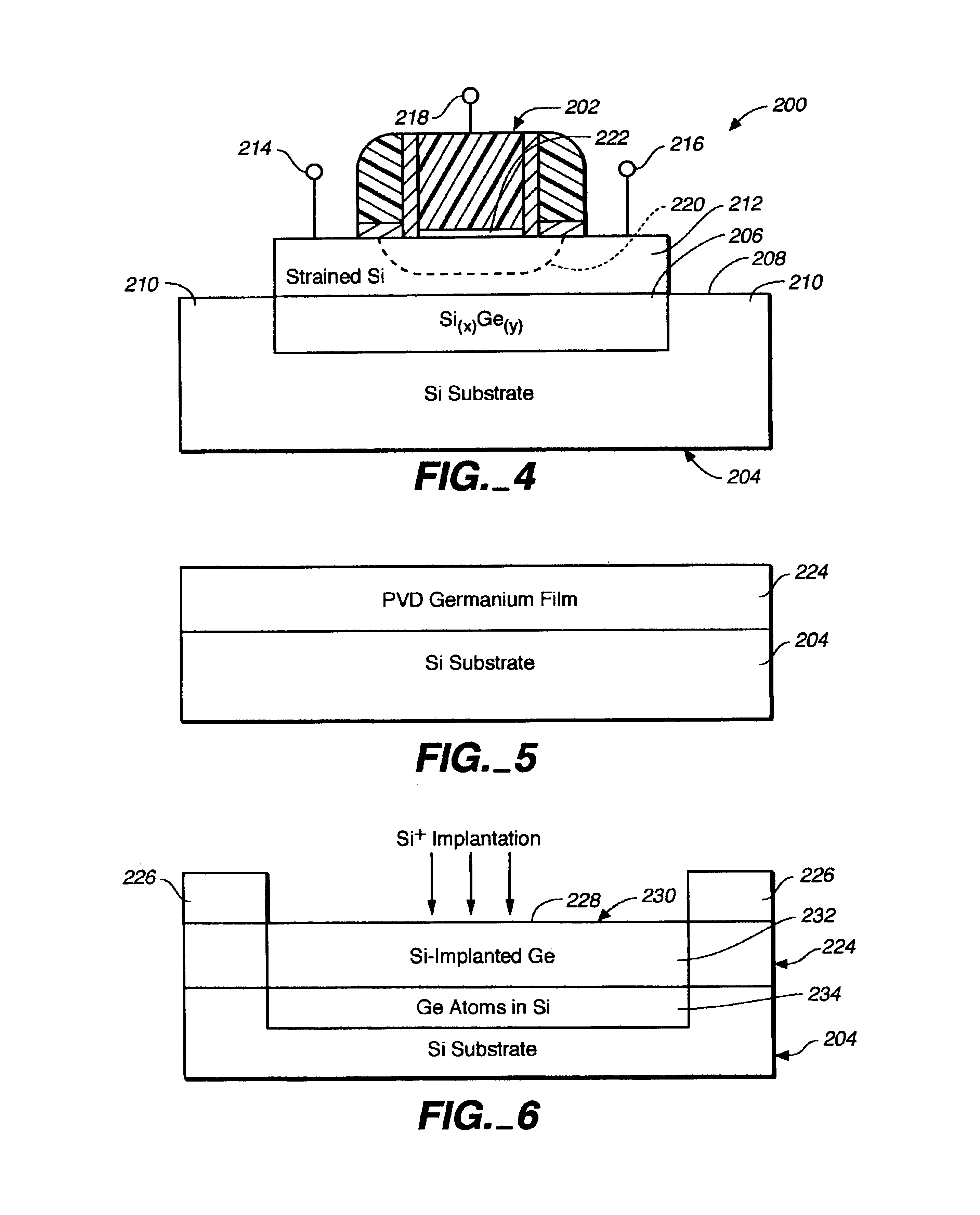
[0020]A portion of an integrated circuit (IC) 200 which incorporates the present invention and which is formed by the methodology of the present invention is shown in FIG. 4. The IC 200 includes a CMOS device 202 (such as a conventional CMOS transistor) formed above a silicon (Si) substrate 204 preferably, but not necessarily, with sub-0.1 micron technology. The Si substrate 204 generally includes an ion-implanted region 206 that extends below the surface 208 of the Si substrate 204. The ion-implanted region 206 is formed by an ion recoil procedure described below. The Si substrate 204 may also include conventional non-implanted regions 210, such as are used with conventional CMOS devices (not shown) and the channel regions thereof. A strained Si region 212 is formed on the ion-implanted region 206 and the CMOS device 202 is formed thereon. The strained Si region 212 is preferably formed by strained Si epitaxial growth or by other strained Si formation techniques. The CMOS device 20...


PUM


Abstract

An integrated circuit (IC) includes a CMOS device formed above a semiconductor substrate having ions therein that are implanted in the semiconductor substrate by an ion recoil procedure. The IC preferably, but not necessarily, incorporates sub-0.1 micron technology in the CMOS device. The implanted ions may preferably be germanium ions. A strained-silicon layer is preferably, but not necessarily, formed above the ion-implanted layer of the semiconductor substrate. The strained-silicon layer may be formed by a silicon epitaxial growth on the ion-implanted layer or by causing the ions to recoil into the semiconductor substrate with such energy that a region of the semiconductor substrate in the vicinity of the surface thereof is left substantially free of the ions, thereby forming a strained-silicon layer in the substantially ion-free region.

Description

CROSS-REFERENCE TO RELATED APPLICATION[0001]This invention is related to an invention for Ion Implantation in Channel Region of CMOS Device for Enhanced Carrier Mobility, described in U.S. patent application Ser. No. 10 / 418,375, which is filed concurrently herewith, invented by the present inventors, and assigned to the assignee of the present invention. The subject matter of this concurrently filed application is incorporated herein by this reference.FIELD OF THE INVENTION[0002]This invention relates to semiconductor integrated circuits (ICs) preferably, but not necessarily, having IC components with sub-0.1 micron dimensions and enhancements to carrier mobility in the channel region of the components. In particular, this invention relates to a new and improved technique for forming a strained-silicon layer for the channel region to enhance carrier mobility in the channel region. In this manner, relatively high performance requirements for CMOS (complimentary metal-oxide semiconduc...

Claims


Application Information

Patent Timeline
Patent Type & Authority Patents(United States)
IPC IPC(8): H01L23/48H01L21/265H01L21/8238H01L29/10
CPCH01L21/26506H01L21/26526H01L29/1054H01L21/823864H01L21/823807
Inventor SUVKHANOV, AGAJANMIRABEDINI, MOHAMMAD R.
Owner BELL SEMICON LLC
Why Eureka
Try Eureka