Semiconductor memory device

a memory device and semiconductor technology, applied in semiconductor devices, digital storage, instruments, etc., can solve the problems of small capacitance, large yield drop, and low yield, so as to reduce the voltage on the word line, static noise margin, and voltage at a low-potential memory node.

Inactive Publication Date: 2006-01-03
PANASONIC CORP
View PDF9 Cites 21 Cited by
  • Summary
  • Abstract
  • Description
  • Claims
  • Application Information

AI Technical Summary

Benefits of technology

[0009]It is therefore an object of the present invention to provide a semiconductor memory device operating with stability even in the case of an SRAM memory cell in which an access transistor and a drive transistor have the same gate width.
[0010]In order to achieve this object, each first and second semiconductor memory devices according to the present invention includes a six-transistor memory cell and also includes a word line and a pair of bit lines connected to the memory cell. In each of the first and second semiconductor memory devices, voltages on the pair of bit lines before read operation of the memory cell are set at a given voltage lower than a power supply voltage. By thus reducing the voltages on the pair of bit lines, the pair of bit lines is at an intermediate potential lower than the power supply voltage when the word line is activated for read operation. Accordingly, out of a high-potential memory node and a low-potential memory node formed in the memory cell, a voltage at the low-potential memory node is reduced lower than that of the prior art. As a result, even if an access transistor and a drive transistor have the same gate width, an apparent current drive capability of the access transistor decreases and a static noise margin increases, thus preventing a malfunction in read operation.
[0013]To achieve the above object, a third semiconductor memory device according to the present invention includes a six-transistor memory cell; and a word line and a pair of bit lines connected to the memory cell, wherein an activation voltage on the word line in read operation of the memory cell is set at a given voltage lower than a power supply voltage. By thus reducing the voltage on the word line, the on-state resistance of an access transistor in read operation is higher than the on-state resistance of a drive transistor, so that the voltage at a low-potential memory node decreases. Accordingly, even if the access transistor and the drive transistor have the same gate width, the static noise margin is large enough to prevent a malfunction in read operation.

Problems solved by technology

In addition, the amount of wasted space is smaller than in the vertical cell structure, so that the memory cell area decreases and the bit line length becomes shorter accordingly, resulting in a small capacitance.
If this voltage rise is too large, a malfunction that the data held in the low-potential memory node changes to high occurs.
As a result, there arise a problem that the static noise margin decreases to cause a malfunction in read operation and thus the yield decreases largely.

Method used


Image

  • Semiconductor memory device
  • Semiconductor memory device
  • Semiconductor memory device

Examples


embodiment 1

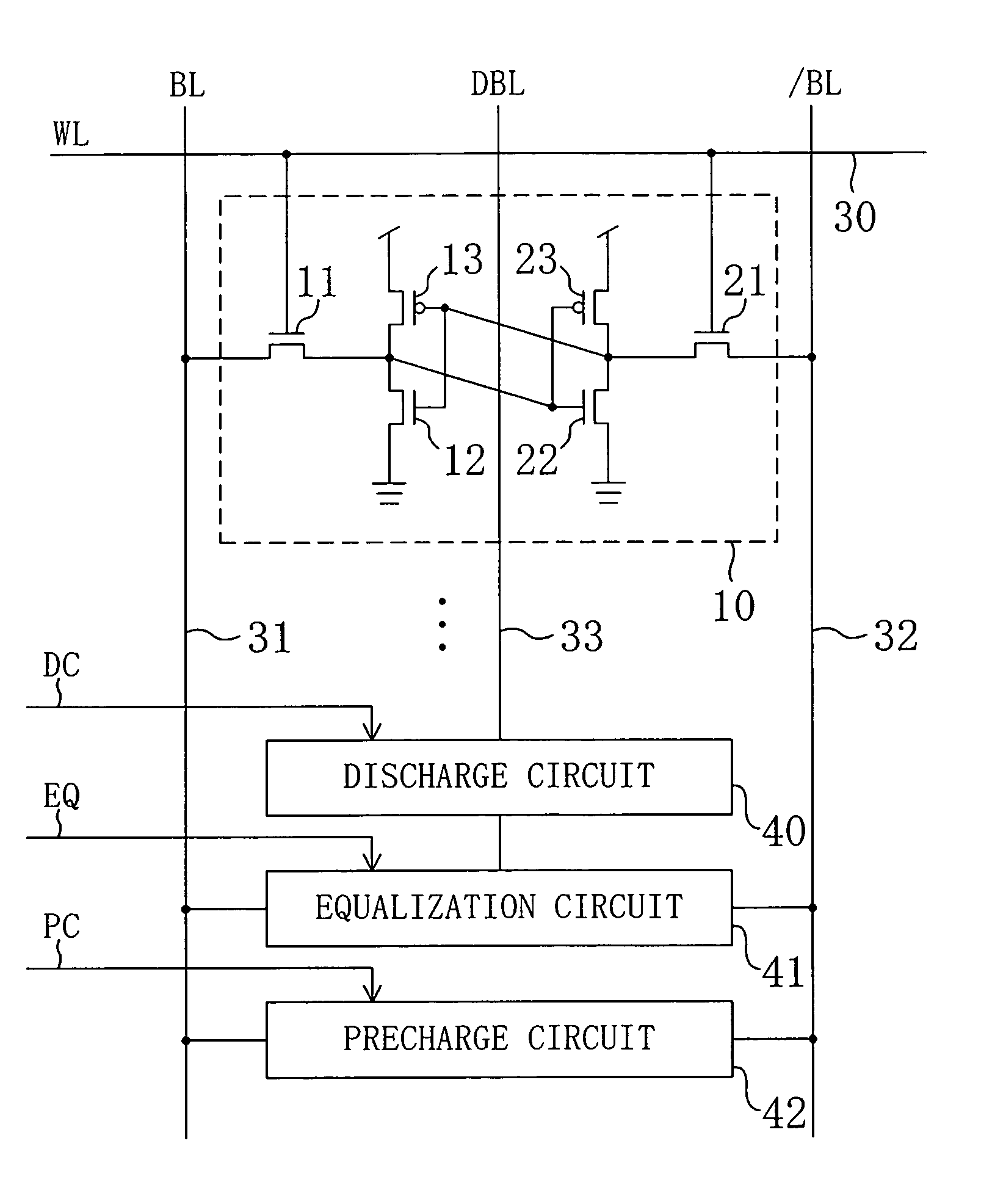
[0027]FIG. 1 shows a configuration of a semiconductor memory device according to a first embodiment of the present invention. In FIG. 1, a memory cell 10 is a six-transistor memory cell including: a pair of NMOS access transistors 11 and 21; a pair of NMOS drive transistors 12 and 22; and a pair of PMOS load transistors 13 and 23. Reference numeral 30 denotes a word line (WL), reference numerals 31 and 32 denote a pair of bit lines (BL and / BL), reference numeral 33 denotes a dummy bit line (DBL), reference numeral 40 denotes a discharge circuit, reference numeral 41 denotes an equalization circuit and reference numeral 42 denotes a precharge circuit. The memory cell 10 is connected to the word line 30 and the pair of bit lines 31 and 32. The discharge circuit 40 is connected to the dummy bit line 33 and receives a discharge control signal DC. The equalization circuit 41 is connected to the pair of bit lines 31 and 32 and the dummy bit line 33 and receives an equalization control si...

embodiment 2

[0037]FIG. 6 shows a configuration of a semiconductor memory device according to a second embodiment of the present invention. The configuration shown in FIG. 6 is different from that of the first embodiment in that a PMOS transistor, for example, is provided as a transistor 43 for electrically dividing a dummy bit line (DBL) 33 into two when a dummy-bit-line adjustment signal DA is at an H level. The other part of the configuration is the same as that of the first embodiment.

[0038]FIG. 7 shows read operation of the semiconductor memory device shown in FIG. 6. According to FIG. 7, when the dummy-bit-line adjustment signal DA is at an L level and the PMOS transistor 43 is activated, the operation is the same as in the first embodiment. On the other hand, when the dummy-bit-line adjustment signal DA is at an H level and the PMOS transistor 43 is inactivated, a small amount of charge moves during equalization in a period T2, so that it is possible to reduce voltage drops on a pair of b...

embodiment 3

[0042]FIG. 8 shows a configuration of a semiconductor memory device according to a third embodiment of the present invention. In the configuration shown in FIG. 8, the discharge circuit 40 of the first embodiment is constituted by a PMOS transistor 44 for drawing charge from a dummy bit line (DBL) 33. A discharge circuit 40 according to this embodiment discharges the dummy bit line 33 to a threshold voltage Vt of the PMOS transistor 44 when a discharge control signal DC is at an L level. Reference sign SC denotes a substrate potential control signal for changing a substrate potential of the PMOS transistor 44. The other part of the configuration is the same as in the first embodiment.

[0043]FIG. 9 shows read operation of the semiconductor memory device shown in FIG. 8. According to the configuration shown in FIG. 8, the threshold voltage Vt of the PMOS transistor 44 is changed with the substrate potential control signal SC. For example, if the threshold voltage Vt is zero (Vt=0), the...


PUM


Abstract

A dummy bit line is provided between a pair of bit lines. The pair of bit lines is set at a power supply voltage and the dummy bit line is set at a ground voltage, and then the pair of bit lines and the dummy bit line are equalized. When a word line is activated in subsequent read operation, the pair of bit lines is at an intermediate potential lower than the power supply voltage, so that an apparent current drive capability of an access transistor decreases, and the static noise margin of a memory cell increases.

Description

BACKGROUND OF THE INVENTION[0001]The present invention relates to a semiconductor memory device, and more particularly relates to a static random access memory (SRAM).[0002]With recent downsizing in semiconductor processing, variation in transistor characteristics has been increasing. This has a large effect on circuit yields, and designs for suppressing the variation in transistor characteristics will become more and more important.[0003]An SRAM memory cell of a six-transistor CMOS type has been known to date. This SRAM memory cell is constituted by three types of transistors (six transistors) in total, i.e., a pair of NMOS access transistors, a pair of NMOS drive transistors and a pair of PMOS load transistors.[0004]To suppress variation in manufacturing SRAM memory cells and to reduce the memory cell area and the bit-line capacitance, a planar cell structure was devised. Unlike a vertical cell structure having an N-well in the upper half of a memory cell region and a P-well in th...

Claims


Application Information

Patent Timeline
Patent Type & Authority Patents(United States)
IPC IPC(8): G11C11/00G11C11/41G11C11/413G11C11/419H01L21/8244H01L27/11
CPCG11C11/419
Inventor SUMITANI, NORIHIKOHOUMURA, SHIGEONAKAI, YOUJIKANEHARA, HIDENARITSUJIMURA, KAZUKI
Owner PANASONIC CORP
Why Eureka
Try Eureka