Method and apparatus for manufacturing known good semiconductor die

a technology of semiconductor dice and manufacturing method, which is applied in the direction of semiconductor/solid-state device testing/measurement, semiconductor/solid-state device details, instruments, etc., can solve the problems of high cost, large time, materials and capital investment for manufacturing packaged dice, and complex process for packaging semiconductor di

Inactive Publication Date: 2006-01-10
MICRON TECH INC
View PDF53 Cites 21 Cited by
  • Summary
  • Abstract
  • Description
  • Claims
  • Application Information

AI Technical Summary

Benefits of technology

[0018]Accordingly, it is an object of the present invention to provide an improved method for manufacturing known good die.
[0020]It is a further object of the present invention to provide an improved method for manufacturing known good die utilizing carriers adapted to test and burn-in a bare, unpackaged die without damage to the die.
[0021]It is a still further object of the invention to provide a method for manufacturing known good die utilizing carriers that are reusable and easy to assemble, that provide a reliable electrical connection with contact locations on a die over a wide temperature range, and that can be easily adapted to testing of different types of dice.
[0022]It is a still further object of the present invention to provide a method and apparatus for manufacturing known good die that are efficient, reliable and suitable for large scale semiconductor manufacture.

Problems solved by technology

This is because the processes for packaging semiconductor dice are extremely complex and costly.
As is apparent, the packaging process (steps 16-40) for manufacturing packaged dice requires a large amount of time, materials and capital investment to accomplish.
A disadvantage of manufacturing unpackaged dice is that transport and testing of the dice is more difficult to accomplish.
The bond pads on a die are particularly susceptible to damage during the test procedure.

Method used


Image

  • Method and apparatus for manufacturing known good semiconductor die
  • Method and apparatus for manufacturing known good semiconductor die
  • Method and apparatus for manufacturing known good semiconductor die

Examples


Embodiment Construction

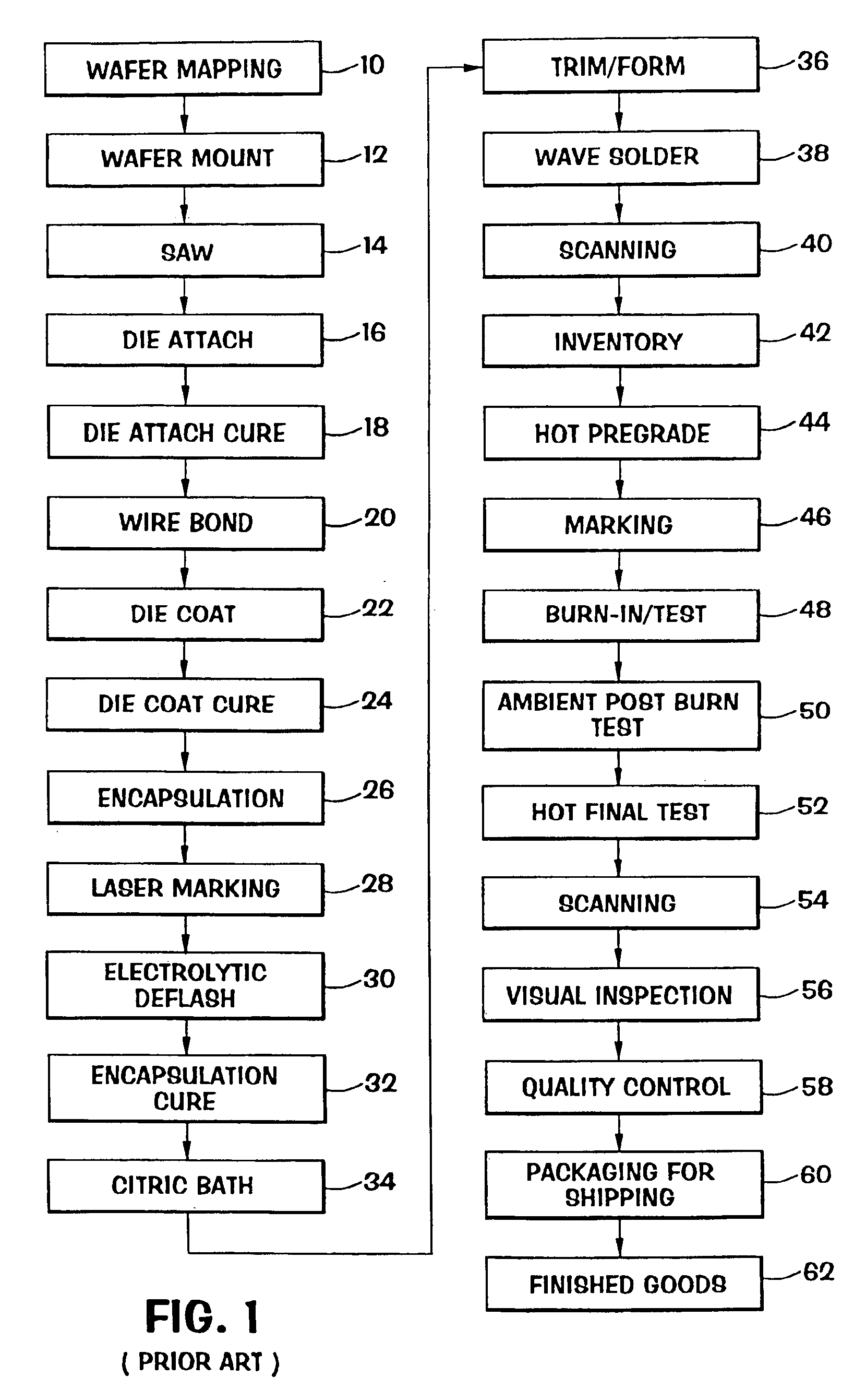
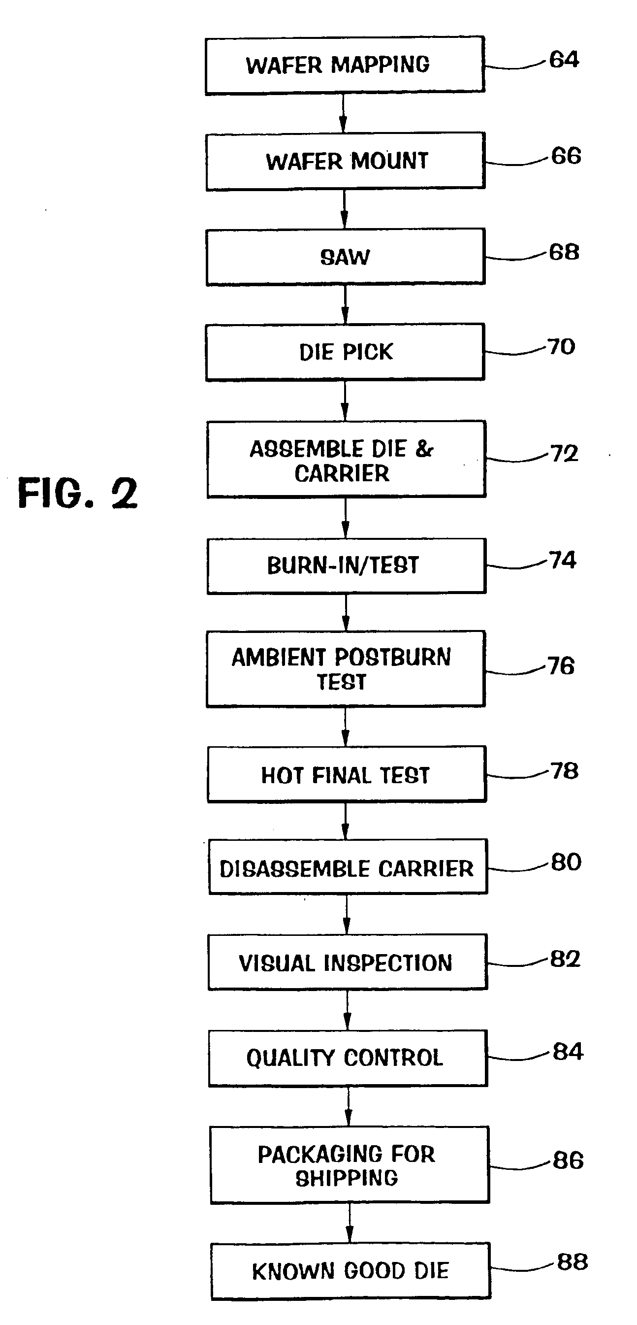
[0045]Referring now to FIG. 2, the method of the invention is illustrated in a flow diagram. During the semiconductor manufacturing process a semiconductor wafer is fabricated with a large number of dice. The wafer is formed by patterning and doping a semiconducting substrate and then depositing, patterning and etching various layers of material on the substrate to form integrated circuits. Initially, the wafer is subjected to probe testing to ascertain the gross functionality of the dice contained on the wafer. Each die is given a brief test for functionality, and the nonfunctional die are mechanically marked or mapped in software, step 64. Wafer probe includes various functional and parametric tests of each die. Test patterns, timing voltage margins, limits and test sequence are determined by individual product yields and reliability data.

[0046]Four testing levels (C1, C2, C3, C7) have been established for semiconductor die. Standard probe (C1) level includes the standard test for...


PUM

PropertyMeasurementUnit
temperatureaaaaaaaaaa
electrical functionality testaaaaaaaaaa
electrical functionalityaaaaaaaaaa

Abstract

A method and apparatus for fabricating known good semiconductor dice are provided. The method includes the steps of: testing the gross functionality of dice contained on a semiconductor wafer; sawing the wafer to singulate a die; and then testing the die by assembly in a carrier having an interconnect adapted to establish electrical communication between the bond pads on the die and external test circuitry. The interconnect for the carrier can be formed using different contact technologies including: thick film contact members on a rigid substrate; self-limiting contact members on a silicon substrate; or microbump contact members with a textured surface. During assembly of the carrier, the die and interconnect are optically aligned and placed into contact with a predetermined contact force. This establishes an electrical connection between the contact members on the interconnect and the bond pads of the die. In the assembled carrier the die and interconnect are biased together by a force distribution mechanism that includes a bridge clamp, a pressure plate and a spring clip. Following testing of the die, the carrier is disassembled and the tested die is removed.

Description

CROSS REFERENCE TO RELATED APPLICATIONS[0001]This application is a continuation of U.S. application Ser. No. 08 / 975,549 filed on Nov. 20, 1997; now U.S. Pat. No. 6,763,578 which is a continuation of U.S. application Ser. No. 08 / 758,657 filed on Dec. 2, 1996; now abandoned which is a continuation of U.S. application Ser. No. 08 / 485,086 filed on Jun. 7, 1995; now U.S. Pat. No. 5,640,762 which is a continuation of U.S. application Ser. No. 08 / 338,345 filed on Nov. 14, 1994, now U.S. Pat. No. 5,634,267 which is a continuation-in-part of application Ser. No. 08 / 073,005 filed on Jun. 7, 1993; now U.S. Pat. No. 5,408,190 which is a continuation-in-part of application Ser. No. 07 / 709,858 filed on Jun. 4, 1991, now abandoned, Ser. No. 07 / 788,065 filed on Nov. 5, 1991, and Ser. No. 07 / 981,956 filed on Nov. 24, 1992.[0002]U.S. application Ser. No. 08 / 485,086 filed on Jun. 7, 1995, is also a continuing application of U.S. application Ser. No. 08 / 338,345 filed on Nov. 14, 1994; which is a contin...

Claims


Application Information

Patent Timeline
Patent Type & Authority Patents(United States)
IPC IPC(8): H05K3/30G01R1/04G01R1/067G01R1/073G01R3/00G01R31/28H01L21/60H01L21/66H01L21/68H01L23/13H01L23/498H05K3/00H05K3/40H05K3/42
CPCG01R1/0433G01R1/0483G01R31/2893H01L21/6835H01L22/20H01L23/13H01L23/49816H01L23/49838H01L24/80H05K3/4007G01R1/0466Y10T29/49117G01R1/06711G01R1/0735G01R3/00G01R31/2863G01R31/287G01R31/2889H01L2224/16145H01L2225/06562H01L2924/01013H01L2924/01029H01L2924/01032H01L2924/01039H01L2924/01077H01L2924/01078H01L2924/01079H01L2924/01082H01L2924/014H01L2924/14H01L2924/15151H01L2924/15174H05K3/0058H05K3/0067H05K3/423H05K2201/0133H05K2201/0347H05K2201/0367H05K2201/0394H05K2201/09481H05K2201/09563H05K2203/0307H05K2203/0723H01L2924/01005H01L2924/01006H01L2924/01033H01L2924/01042H01L2924/01074H01L2924/10253Y10T29/4913Y10T29/49121Y10T29/49131Y10T29/49126H01L2924/00H01L2224/05571H01L2224/05573H01L2924/00014H01L2924/12042H01L2224/05599
Inventor FARNWORTH, WARRENWOOD, ALAN
Owner MICRON TECH INC
Why Eureka
Try Eureka