Semiconductor device with high structural reliability and low parasitic capacitance

a technology of low parasitic capacitance and high structural reliability, applied in the direction of semiconductor devices, electrical devices, transistors, etc., can solve the problems of increasing chip cost, lowering production yield, increasing chip area, etc., and achieving high performance, preventing damage upon bonding, and moderating the accuracy of aligning margins

Inactive Publication Date: 2006-01-10
RENESAS ELECTRONICS CORP
View PDF5 Cites 6 Cited by
  • Summary
  • Abstract
  • Description
  • Claims
  • Application Information

AI Technical Summary

Benefits of technology

[0012]The present invention intends to provide a high performance semiconductor device, capable of moderating the accuracy for the aligning margin upon back side fabrication step, preventing destruction upon bonding caused by pressure elevation in the inside of a via hole and preventing chip destruction caused by occurrence and extension of cracks.
[0015]This can moderate the accuracy for alignment margin, as well as a region in which the thin semiconductor layer remains is removed to prevent occurrence of cracks. Further, by the provision of an opening reaching the via hole to the surface protection insulating film for connecting the substrate and the transistor region, solvent vapors from the adhesives in the via hole can be released to avoid pressure increase in the via hole.
[0016]Further, according to the semiconductor device of the invention, a semiconductor device of obtaining electrode contact to the semiconductor at the lowermost layer by way of a via hole from the back side can be manufactured easily with a large alignment margin, as well as chip destruction by cracking can be prevented.

Problems solved by technology

However, when mesa etching is conducted for the device isolation as described above in the structure of prior art 1, production yield is lowered when the via hole and the mesa etching region are not aligned strictly at the back side etching step of forming a via hole from the back side in the inside of a transistor region to dispose a conduct region of the emitter electrode.
Further, when a large alignment margin is taken in order to avoid lowering of the yield, the chip area is increased to increase the chip cost.
Further, this results in a structure of leaving a thin semiconductor layer of about several μm or less at the largest to a portion near the electrode contact region, and stresses upon chip bonding such as by pressure increase in the via hole are concentrated in the thin semiconductor region, and induce cracks of crystals, which extend as far as the transistor region tending to cause failure due to chip destruction or transistor destruction.

Method used


Image

  • Semiconductor device with high structural reliability and low parasitic capacitance
  • Semiconductor device with high structural reliability and low parasitic capacitance
  • Semiconductor device with high structural reliability and low parasitic capacitance

Examples


first embodiment

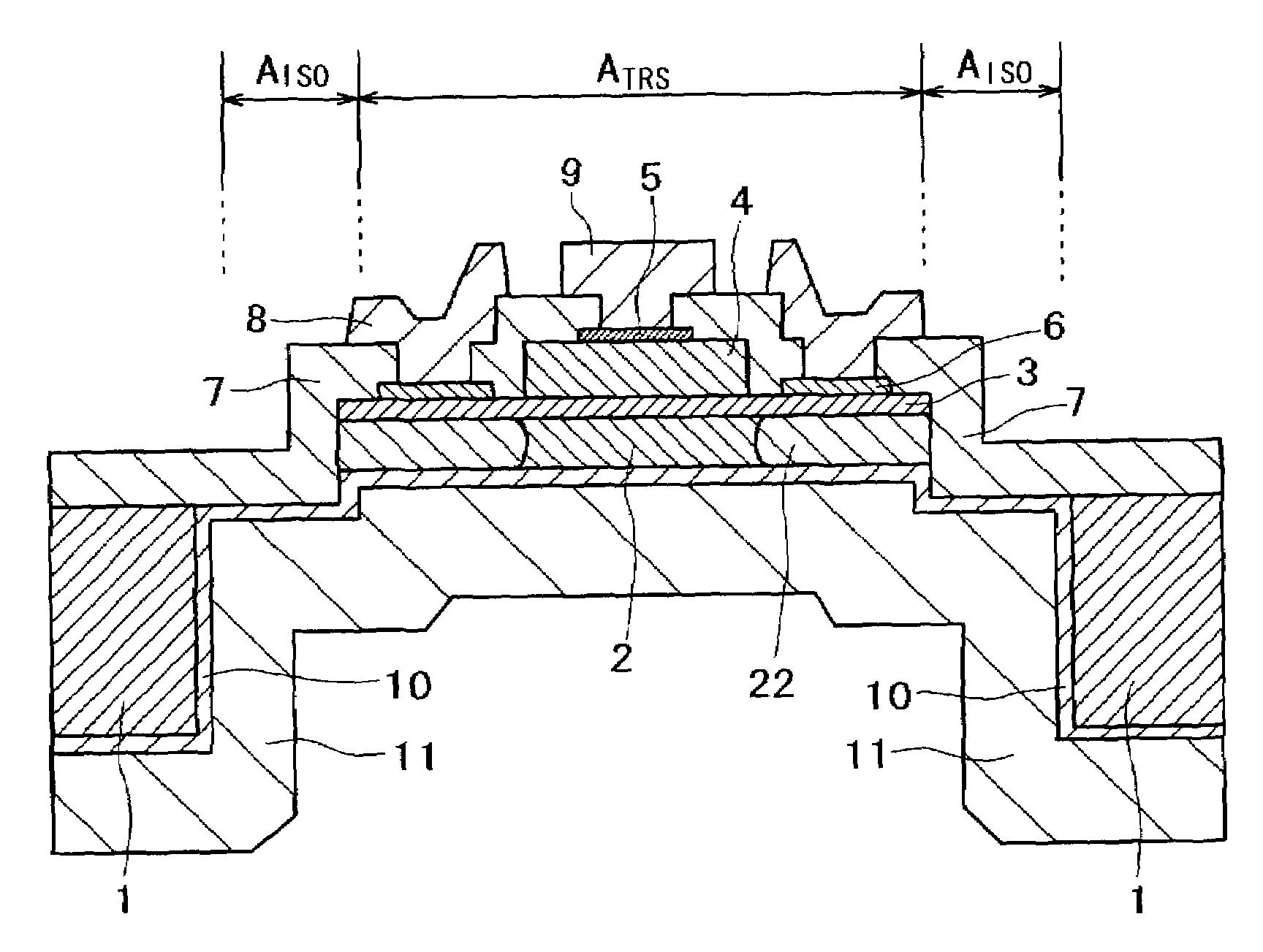
[0039]FIG. 1 shows an example of the semiconductor device, in accordance with the present invention. In FIG. 1, are shown, by reference numerals, a semi-insulating GaAs substrate 1, an emitter layer 2, a base layer 3, a collector layer 4, a collector electrode 5, a base electrode 6, a surface protection insulating film 7 made of SiO2, a base wiring metal 8, a collector wiring metal 9, an emitter electrode 10, an emitter wiring metal 11 formed over the entire back side, and an emitter damaged region 22, respectively. In FIG. 1, ATRS is a transistor region which is occupied by the emitter layer 2. The transistor region ATRS also includes a damaged region 22.

[0040]In this embodiment, the opening of a via hole opened to the substrate 1 from the back side is wider than the transistor region ATRS, the emitter region 2 and the substrate 1 are isolated and connected by the surface protection insulating film 7, the emitter electrode 10 and the emitter wiring metal 11.

[0041]Then, a method of ...

embodiment 1

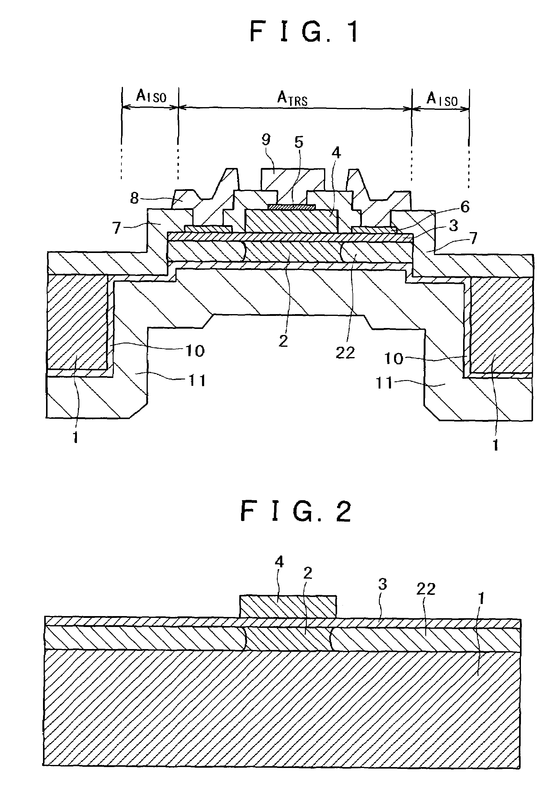
[0073]FIG. 12 shows a schematic cross sectional structural view of a semiconductor device of the invention. This is different described above in that the GaAs substrate 1 is removed over the entire back side.

[0074]The structure can be obtained by forming the insulating film of the surface protection film 7 formed in the step (5) of Embodiment 1 with a polyimide layer 70 (coated to 1 μm thickness and cured at 300° C. in a nitrogen ambient), and removing the GaAs substrate 1 over the entire back side without patterning by photolithography upon etching from the back side in the step (8).

[0075]The feature of the structure resides in that since the GaAs substrate is removed completely and the transistor region is left in an island shape in an extremely thin structure of about 10 μm thickness comprising a polyimide film 70 and an emitter electrode 10 and emitter wirings 11 of the metal layer, the structure has flexibility. Therefore, the transistor of this embodiment can be bonded directl...

embodiment 5

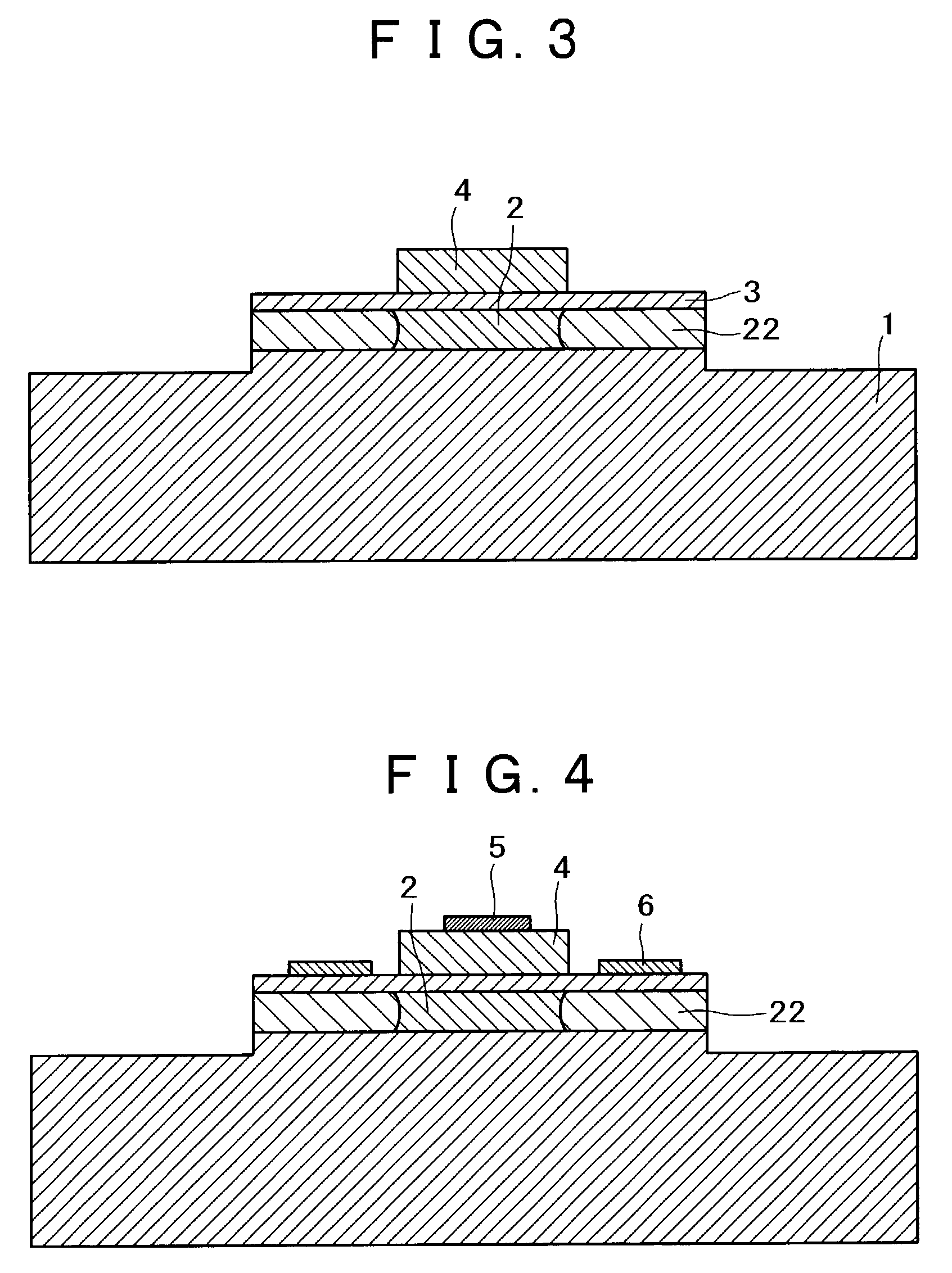
[0077]FIG. 13 shows a schematic cross sectional structural view and FIG. 14 shows a schematic planar structural view of The manufacturing steps of this embodiment are as described below.

[0078]In Embodiment 1 described above, a step of fabricating a surface protection insulating film 7 is conducted between the step (7) and the step (8) and, finally, the semiconductor substrate is removed and openings 40 are formed as shown in FIG. 13 in a region where the transistor region and the substrate region are connected by the surface protection layer. FIG. 14 is a schematic structural plan view showing the same on the side of the surface. FIG. 13 is a cross sectional view for a portion taken along line A–A′ in FIG. 14. In the plan view of FIG. 14, the collector wirings 9 and the base wirings 8 are not illustrated for making the structure clearer.

[0079]In the succeeding step (9), a step of covering the openings 40 with a photoresist upon depositing an emitter electrode is added. Au is no mor...


PUM


Abstract

A semiconductor device with high structural reliability and low parasitic capacitance is provided. In one example, the semiconductor device has a surface. The semiconductor device comprises a semiconductor region, wherein an emitter region, a base region, and a collector region are laminated from a side near a substrate of the semiconductor region; an insulating protection layer disposed on the surface; and a wiring layer disposed on the surface, the insulating protection layer forming a via hole from the side of the substrate of the semiconductor region, the via hole being formed to allow the wiring layer to make a contact to an electrode of the emitter region from a side of the substrate where the emitter region, the base region, and the collector region are laminated and where the semiconductor region is isolated.

Description

COPYRIGHT NOTICE[0001]A portion of the disclosure of this patent document contains material which is subject to copyright protection. The copyright owner has no objection to the facsimile reproduction by anyone of the patent document or the patent disclosure, as it appears in the Patent and Trademark Office patent file or records, but otherwise reserves all copyright rights whatsoever.BACKGROUND OF THE INVENTION[0002]1. Field of the Invention[0003]The present invention generally relates to a semiconductor device of excellent high frequency operation and, more particular, to a semiconductor device having high structural reliability while reducing the parasitic capacitance as low as possible.[0004]2. Discussion of Background[0005]As a structure of an existing semiconductor device of excellent high frequency operation, a hetero-junction bipolar transistor disclosed in JP-A No. 177966 / 1987 (prior art 1) has been known. In the device structure of the prior art 1, an emitter layer compris...

Claims


Application Information

Patent Timeline
Patent Type & Authority Patents(United States)
IPC IPC(8): H01L27/082H01L21/331H01L29/06H01L29/417H01L29/737
CPCH01L29/0657H01L29/0692H01L29/41708H01L29/66318H01L29/7371H01L24/32H01L2924/1305H01L2924/00H01L2924/15787
Inventor TANOUE, TOMONORIMOCHIZUKI, KAZUHIROYAMADA, HIROJI
Owner RENESAS ELECTRONICS CORP
Why Eureka
Try Eureka