Supercharge Your Innovation With Domain-Expert AI Agents!

E-beam curable resist and process for e-beam curing the resist

Inactive Publication Date: 2006-01-24
APPLIED MATERIALS INC
View PDF17 Cites 4 Cited by
  • Summary
  • Abstract
  • Description
  • Claims
  • Application Information

AI Technical Summary

Problems solved by technology

As a result, the resolution capacity that can be obtained with conventional UV microlithography has its limits, and in order to sufficiently resolve optically small structural elements, wavelengths shorter than UV radiation must be utilized.
However, UV photoresist materials used today are not suitable for use with radiation at wavelengths of 157 nm, 193 nm or 248 nm.
This is because materials based on phenolic resins as a binding agent (particularly novolak resins or polyhydroxystyrene derivatives) have too high an absorption at such wavelengths, and cannot be imaged through films of the thicknesses needed to fabricate ICs (for example, polyhydroxystyrene based photoresists can be used in top surface imaging applications in which only a very thin (˜500 Å) layer of photoresist is required to be transparent at the wavelength of an ArF laser, i.e., λ˜193 nm).
Such high absorption results in side walls of developed photoresist structures that do not form vertical profiles.
Rather the side walls form an oblique angle with respect to the substrate, and this causes poor optical resolution characteristics at these short wavelengths.
These protecting groups are usually very large, or bulky, molecules that are attached to the resin via bonds that can be easily cleaved.
However, there are problems associated with such chemically amplified photoresists.
One problem is that such photoresists lack sufficient etch resistance, thermal stability, post exposure delay stability, and processing latitude to useful for fabricating ICs.
In particular, while such photoresists are sufficiently transparent for deep UV radiation, they do not have the required etch resistance with respect to plasma etching that is evidenced by photoresists based on phenolic resins.
This issue is compounded by the fact that the thickness of the photoresist is limited by pattern collapse issues at high aspect ratios, and the limited depth of focus of, for example, and without limitation, 193 nm photolithography tools.
However, lower photoresist thickness exacerbates the issue of etch resistance.
Another problem is that, after optical exposure and completion of the de-protection reactions, the photoresist in the exposed areas can shrink from ten to twenty percent.
This is believed to be due to the loss of the bulky protecting groups as volatiles.
Thus, since the unexposed photoresist still contains resin with attached blocking groups, it is susceptible to shrinkage if these molecules are removed.
This happens at different temperatures for different protection groups, but can be at a temperature as low as 40° C. to a temperature as high as 200° C. Thus, thermal activation may result in loss of blocking groups as volatiles, and a resulting shrinkage of the photoresist.
This reaction cleaves the link between the protecting groups and the resin, results in shrinkage of the photoresist.
Since the full thickness of the photoresist is targeted for etch stabilization, substantial mass loss, and shrinkage, can result from the electron beam exposure.
The pullback phenomenon has undesired effects on features, which make them unacceptable for device fabrication.
However, due to the volatility of additives in the disclosed photoresist materials, electron beam exposure causes expulsion of these additives, which, in turn, causes shrinking of the photoresist.
However, this is problematic because the use of metal-containing reagents introduce undesirable contaminants which are difficult to remove using conventional stripping procedures.

Method used


Image

  • E-beam curable resist and process for e-beam curing the resist
  • E-beam curable resist and process for e-beam curing the resist
  • E-beam curable resist and process for e-beam curing the resist

Examples


Embodiment Construction

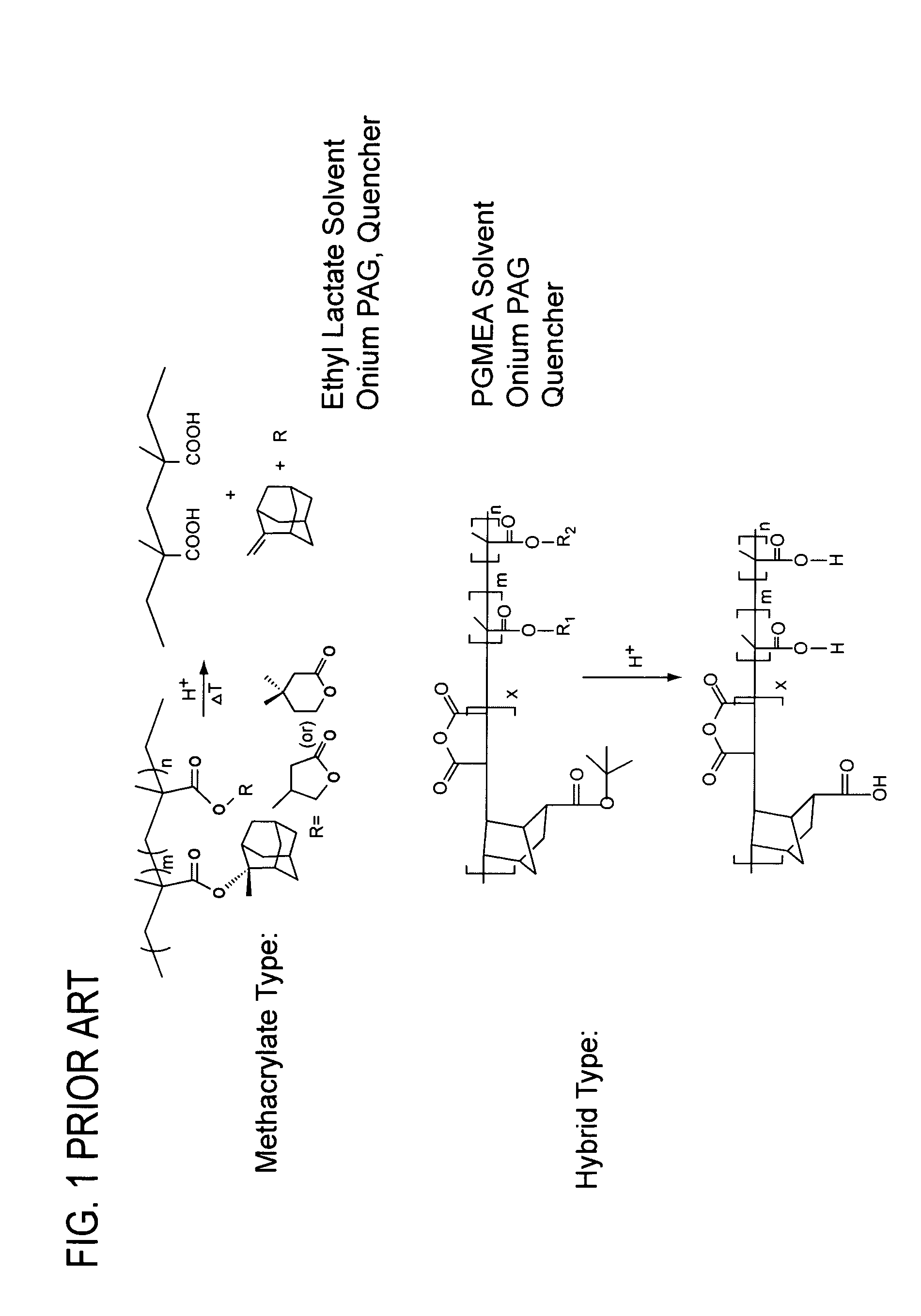
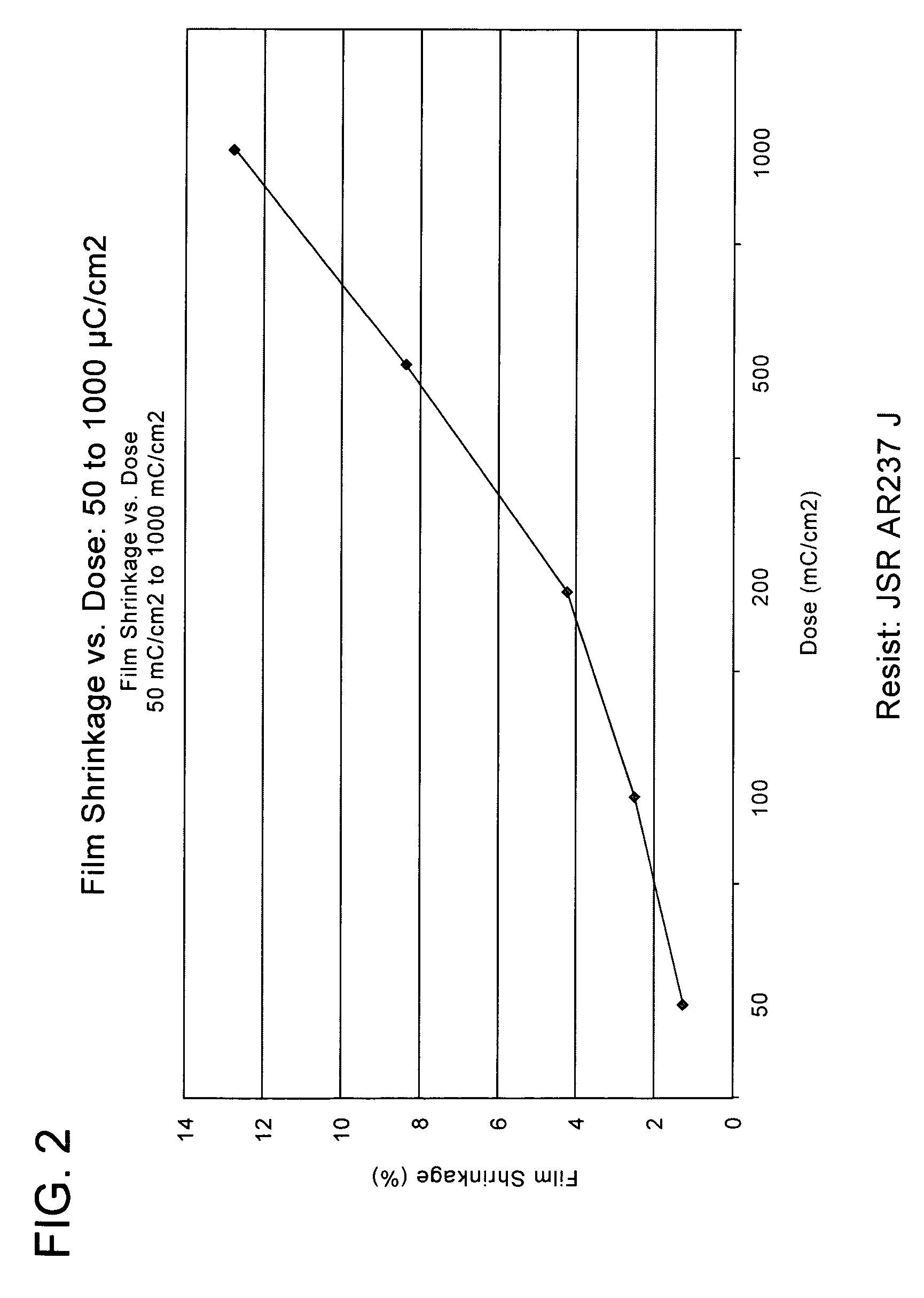
[0024]One or more embodiments of the present invention provide one or more of the following advantages: (a) elimination, or reduction, of photoresist film shrinkage and pull-back after electron beam (“e-beam”) treatment; (b) elimination, or reduction, of the loss of volatile materials during e-beam treatment (i.e., materials that leave the photoresist film resulting in film shrinkage, and / or contamination of an e-beam treatment chamber); and (c) reduction of e-beam treatment doses required to increase its etch resistance, thereby reducing ablation of photoresist components (which ablation leads to shrinkage).

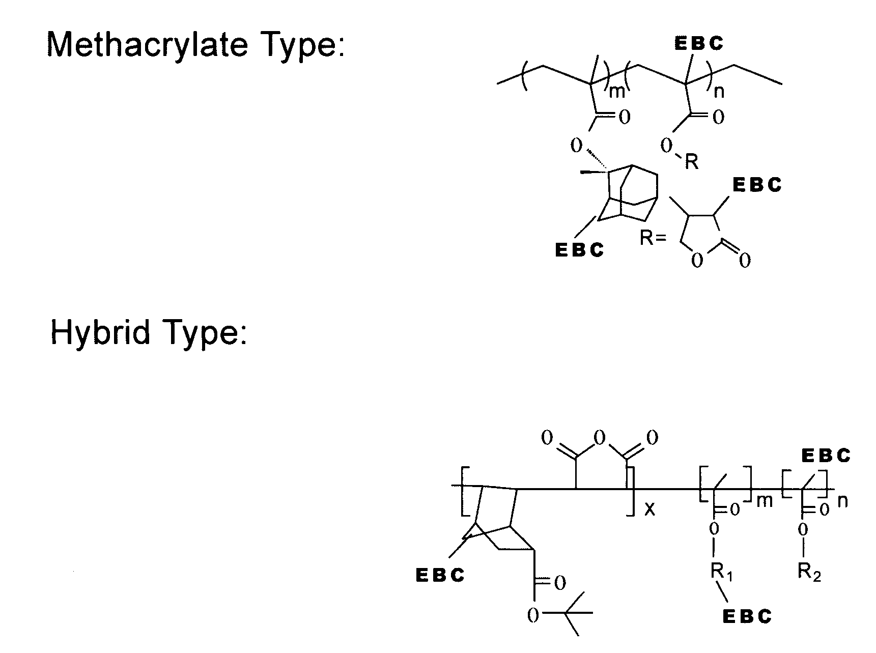
[0025]One or more embodiments of the present invention is a photoresist formulation that includes e-beam cross-linkable substituents that include the following characteristics: (a) the e-beam cross-linkable substituents provide little or no increase in absorption at a particular exposure wavelength used for patterning relative to typical prior art formulations (for example, a tr...


PUM


Abstract

One embodiment of the present invention is a photoresist formulation that includes e-beam cross-linkable substituents, which substituents include one or more of the following functional groups: (a) carbon-carbon double bonds; (b) a strained ring system; (c) a halogenated compound; and (d) one or more organo-silicon moieties.

Description

[0001]This application claims the benefit of U.S. Provisional Application No. 60 / 386,966, filed on Jun. 7, 2002 which application is incorporated herein by reference.TECHNICAL FIELD OF THE INVENTION[0002]One or more embodiments of the present invention relate to photoresist formulations used to fabricate electronic devices such as integrated circuits (“ICs”), and method and apparatus to stabilize such photoresist formulations. In particular, one or more embodiments of the present invention relate to methods and apparatus for increasing the etch resistance of photoresists that are suitable for use in fabricating electronic devices such as ICs. In further particular, one or more embodiments of the present invention relate to a method for increasing the etch resistance of positive working, chemically amplified, photoresists such as, for example, and without limitation, 193 nm, 157 nm, deep-UV (248 nm), x-ray sensitive, and electron beam sensitive resists while improving and maintaining...

Claims


Application Information

Patent Timeline
IPC IPC(8): G03F7/075G03F7/027G03F7/40G03F7/039G03F7/38G03F7/20
CPCG03F7/0392G03F7/40G03F7/2024G03F7/2059
Inventor WEIDMAN, TIMOTHYLIVESAY, WILLIAM R.ROSS, MATTHEW F.
Owner APPLIED MATERIALS INC
Features
  • R&D
  • Intellectual Property
  • Life Sciences
  • Materials
  • Tech Scout
  • Unparalleled Data Quality
  • Higher Quality Content
  • 60% Fewer Hallucinations
Learn More